

| Distributor | Stock | Pricing | MOQ | PKG | Lead Time | Date Code | On Order Quantity | On Order Delivery | |
|---|---|---|---|---|---|---|---|---|---|
|
22,600 pcs
|
22600 pcs | On Request | 1 | On Request | On Request | On Request | On Request | On Request |
| Category | |
| Manufacturer Name | |
| AEC Qualified | |
| Automotive Grade | |
| Differential | |
| Divider | |
| Frequency | |
| Halogen Free | |
| Industrial Grade | |
| Input | |
| Medical Grade | |
| Military Grade | |
| Mounting Type | |
| Number of Circuits | |
| Operating Temperature | |
| Operating Voltage | |
| Output | |
| PLL | |
| Quiescent Current | |
| Ratio | |
| SVHC Present | |
| Supplier Device Package | |
| Tape & Reel | |
| Type | |
| Voltage |
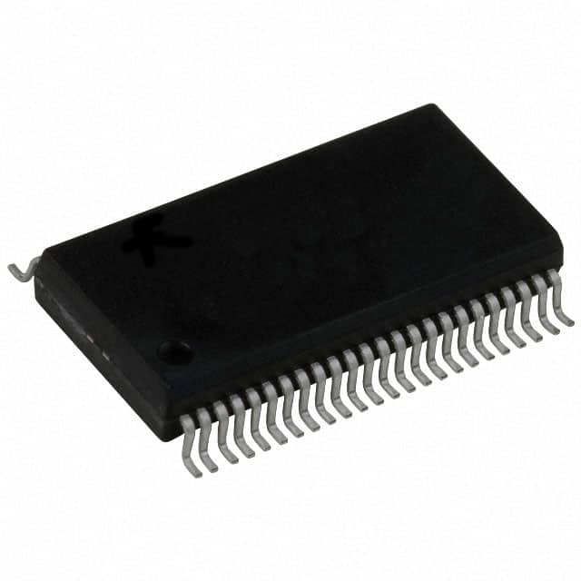
The Texas Instruments CDCV857DGGR is a high-performance, low-skew, low-jitter zero delay buffer designed for Double Data-Rate Synchronous DRAM applications. It distributes one differential clock input to ten differential outputs and one feedback clock output.
Key electrical specifications include an operating frequency range of 60 to 200 MHz and a cycle-to-cycle jitter of ±75 ps. The device operates from dual 2.5-V supplies and consumes less than 200-mA quiescent current. It features a PLL with bypass capability and supports differential clock inputs and outputs.
The CDCV857DGGR is housed in a 48-TSSOP package and supports surface mount mounting type. It is characterized for operation from 0°C to 85°C. The device can track spread spectrum clocking for reduced EMI.
The operating frequency range is 60 MHz to 200 MHz.
The cycle-to-cycle jitter is ±75 ps.
The operating voltage is between 2.3 V and 2.7 V.
The package type is 48-TSSOP.
The operating temperature range is 0°C to 85°C.