

| Distributor | Stock | Pricing | MOQ | PKG | Lead Time | Date Code | On Order Quantity | On Order Delivery | |
|---|---|---|---|---|---|---|---|---|---|
|
20,312 pcs
|
20312 pcs | On Request | 1 | On Request | On Request | 1928+ | On Request | On Request | |
|
59 pcs
|
59 pcs | On Request | 1 | On Request | On Request | On Request | On Request | On Request |
| Category | |
| Manufacturer Name | |
| Differential | |
| Divider | |
| Frequency | |
| Input | |
| Input Type | |
| Lead Style | |
| Mounting Type | |
| Number of Circuits | |
| Operating Temperature | |
| Output | |
| PLL | |
| Quiescent Current | |
| Ratio | |
| Supplier Device Package | |
| Type | |
| Voltage |
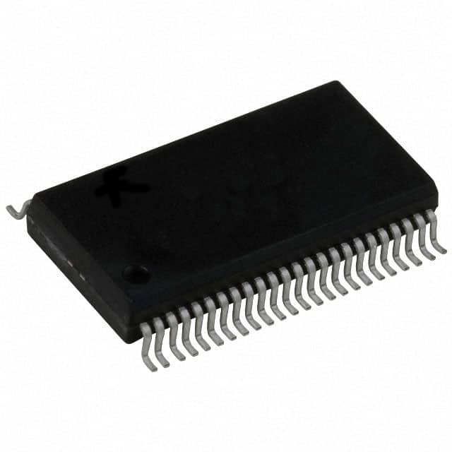
The Texas Instruments CDCV857BIDGG is a high-performance, low-skew, low-jitter PLL Clock Driver. It is designed to distribute one differential clock input to 10 differential outputs and one differential feedback clock output.
This device operates from dual 2.5V supplies and supports a frequency range of 60 MHz to 200 MHz. It offers low jitter with cycle-to-cycle jitter of ±50 ps and period jitter of ±35 ps. The static phase offset is also ±50 ps. The CDCV857BIDGG features a PLL with bypass capability and can track spread spectrum clocking for reduced EMI.
It enters a low-power mode when no CLK input signal is applied or when PWRDWN is low. The device is available in a 48-pin TSSOP package and operates within an industrial temperature range of -40°C to 85°C. It meets or exceeds the latest DDR JEDEC specification JESD82-1.
The CDCV857BIDGG is suitable for Double Data-Rate Synchronous DRAM applications requiring precise clock distribution with minimal jitter and phase offset.
The CDCV857BIDGG operates from 2.3V to 2.7V, with a nominal voltage of 2.5V.
The operating temperature range for the CDCV857BIDGG is -40°C to 85°C.
The CDCV857BIDGG is available in a 48-TSSOP package.
The CDCV857BIDGG is RoHS3 Compliant.
The operating frequency range for the CDCV857BIDGG is 60 MHz to 200 MHz.
The cycle-to-cycle jitter for the CDCV857BIDGG is ±50 ps.