

| Distributor | Stock | Pricing | MOQ | PKG | Lead Time | Date Code | On Order Quantity | On Order Delivery | |
|---|---|---|---|---|---|---|---|---|---|
|
311 pcs
|
311 pcs | On Request | 1 | On Request | On Request | 07+ | On Request | On Request |
| Category | |
| Manufacturer Name | |
| Differential | |
| Divider | |
| Frequency | |
| Input | |
| Mounting Type | |
| Number of Circuits | |
| Operating Temperature | |
| Operating Voltage | |
| Output | |
| PLL | |
| Ratio | |
| Supplier Device Package | |
| Type | |
| Voltage |
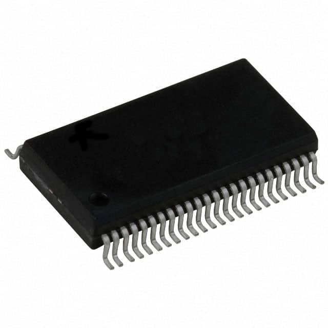
The CDCV857ADGGRG4 from Texas Instruments is a PLL Clock Driver integrated circuit. It is designed for clock generation and distribution within electronic systems. This device features a supply voltage range of 2.3V to 2.7V and can handle a maximum input clock frequency of 180MHz.
The CDCV857ADGGRG4 supports a 1:10 output ratio and offers differential input and output capabilities. It is housed in a 48-TSSOP package, suitable for surface mount applications. The operating temperature range for this component is 0°C to 85°C.
This PLL Clock Driver is part of the broader category of Clock Generators, PLLs, and Frequency Synthesizers. Its design with bypass functionality and specific voltage requirements makes it suitable for various timing-critical applications where precise clock signals are essential.
The device operates within a voltage range of 2.3V to 2.7V.
It is packaged in a 48-TFSOP (0.240 inch, 6.10mm width) surface-mount package.
The maximum input frequency supported is 180MHz.
It operates within a temperature range of 0°C to 85°C.
RoHS compliance status is unverified; treat as low-confidence.