

| Distributor | Stock | Pricing | MOQ | PKG | Lead Time | Date Code | On Order Quantity | On Order Delivery | |
|---|---|---|---|---|---|---|---|---|---|
|
804 pcs
|
804 pcs | On Request | 1 | On Request | On Request | 12+ | On Request | On Request |
| Category | |
| Manufacturer Name | |
| Differential | |
| Divider | |
| Frequency | |
| Input | |
| Lead Style | |
| Mounting Type | |
| Number of Circuits | |
| Operating Temperature | |
| Output | |
| PLL | |
| Quiescent Current | |
| Ratio | |
| Supplier Device Package | |
| Type | |
| Voltage |
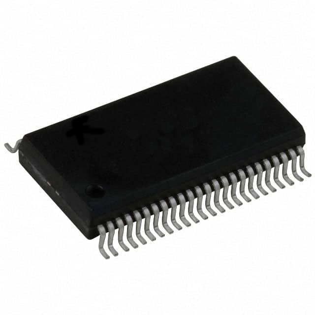
The CDCV857ADGGR from Texas Instruments is a high-performance, low-skew, low-jitter phase-lock loop (PLL) clock driver. It is designed to distribute one differential clock input to ten differential clock outputs, making it suitable for double data-rate synchronous DRAM applications.
This device operates from dual 2.5-V supplies and supports spread spectrum clocking. Key electrical specifications include an operating frequency range of 60 to 180 MHz, an output skew of 75 ps, and a cycle-to-cycle jitter of ±50 ps. The quiescent current is less than 200 uA.
The CDCV857ADGGR features three-state outputs that disable when input differential clocks fall below 20 MHz, entering a low power mode. It is available in a 48-pin TSSOP package, suitable for surface mount applications. The operating temperature range is from 0°C to 85°C.
This clock driver is part of Texas Instruments' clock buffer offerings and is identified by its part number CDCV857A.
| Qty | Low | High |
|---|---|---|
| 1+ | $5.06 | $5.06 |
Estimated market price range - modelled values for guidance only, not live distributor offers.
The CDCV857ADGGR operates from 2.3V to 2.7V.
The CDCV857ADGGR is available in a 48-TSSOP package and a 48-TFSOP (0.240", 6.10mm Width) package.
The operating temperature range for the CDCV857ADGGR is 0°C to 85°C.
The CDCV857ADGGR is RoHS3 Compliant.
The CDCV857ADGGR has a maximum operating frequency of 180 MHz.
The output skew for the CDCV857ADGGR is 75 ps.
The cycle-to-cycle jitter of the CDCV857ADGGR is ±50 ps.