

| Distributor | Stock | Pricing | MOQ | PKG | Lead Time | Date Code | On Order Quantity | On Order Delivery | |
|---|---|---|---|---|---|---|---|---|---|
|
35 pcs
|
35 pcs | On Request | 1 | On Request | On Request | On Request | On Request | On Request | |
|
6 pcs
|
6 pcs | On Request | 1 | On Request | On Request | 09+ | On Request | On Request |
| Category | |
| Manufacturer Name | |
| Differential | |
| Divider | |
| Frequency | |
| Halogen Free | |
| Input | |
| Lead Spacing | |
| Lead Style | |
| Mounting Type | |
| Number of Circuits | |
| Operating Temperature | |
| Output | |
| PLL | |
| Ratio | |
| Supplier Device Package | |
| Type | |
| Voltage | |
| Voltage Supply |
The CDCV855PWG4 from Texas Instruments is a Phase-Locked Loop (PLL) Clock Driver integrated circuit. It is designed for applications requiring precise clock signal generation and distribution, operating at a maximum frequency of 180MHz.
This device features a supply voltage range of 2.3V to 2.7V and an operating temperature range of 0°C to 70°C, making it suitable for various electronic systems. The CDCV855PWG4 supports SSTL-2 input and output standards and offers a 1:5 input to output ratio with differential signaling capabilities.
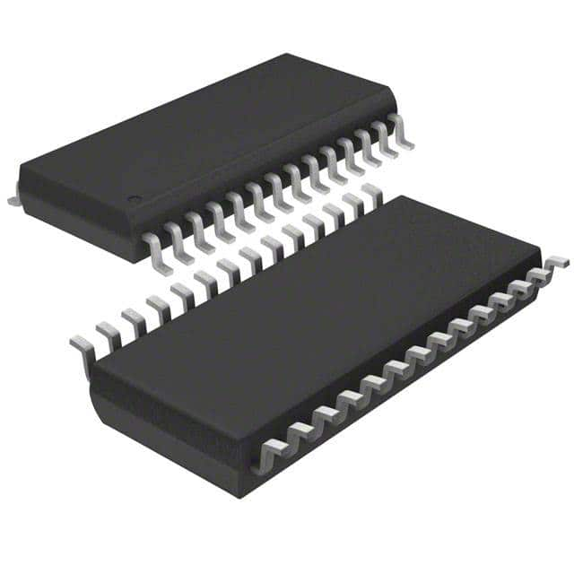
Packaged in a 28-TSSOP (0.173", 4.40mm Width) format, this IC is designed for surface mount applications. Its robust design and specifications make it a reliable choice for clocking solutions in digital systems.
The maximum operating frequency is 180MHz.
The supply voltage range is 2.3V to 2.7V.
The operating temperature range is 0°C to 70°C.
The CDCV855PWG4 is available in a 28-TSSOP package.
Yes, it supports differential input and output.
The input and output standards are SSTL-2.