

| Distributor | Stock | Pricing | MOQ | PKG | Lead Time | Date Code | On Order Quantity | On Order Delivery | |
|---|---|---|---|---|---|---|---|---|---|
|
6,215 pcs
|
6215 pcs | On Request | 1 | On Request | On Request | On Request | On Request | On Request | |
|
5,415 pcs
|
5415 pcs | On Request | 1 | On Request | On Request | On Request | On Request | On Request | |
|
2,829 pcs
|
2829 pcs | On Request | 1 | On Request | On Request | 1822+ | On Request | On Request |
| Category | |
| Manufacturer Name | |
| Differential | |
| Frequency | |
| Input | |
| Input Type | |
| Mounting Type | |
| Number of Circuits | |
| Operating Temperature | |
| Output | |
| Ratio | |
| Supplier Device Package | |
| Supplier Package | |
| Supply Voltage | |
| Type | |
| Voltage |
The CDCV304TPWREP from Texas Instruments is a versatile clock buffer designed for general-purpose and PCI-X applications. It efficiently distributes a single input clock signal (CLKIN) to a bank of four outputs (1Y[0:3]).
This buffer operates at frequencies up to 200 MHz and features a low output skew of less than 100 ps, ensuring signal integrity. It supports supply voltages of 2.5 V and 3.3 V, making it compliant with 3.3-V PCI-X specifications. The device is characterized for operation within an extended temperature range of -40°C to 105°C.
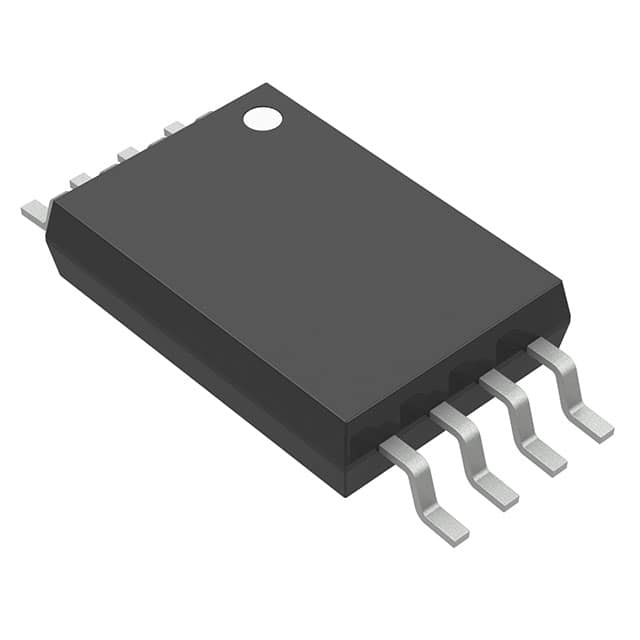
Packaged in an 8-pin TSSOP, the CDCV304TPWREP is suitable for surface mount applications. Its output enable control allows outputs to be driven low when the OE pin is low, providing additional control over signal distribution. This component is ideal for applications requiring reliable clock distribution in demanding environments.
| Qty | Low | High |
|---|---|---|
| 1+ | $5.35 | $5.35 |
Estimated market price range - modelled values for guidance only, not live distributor offers.
The CDCV304TPWREP operates at frequencies up to 200 MHz.
The output skew for the CDCV304TPWREP is less than 100 ps.
The CDCV304TPWREP supports supply voltages of 2.5V and 3.3V.
The CDCV304TPWREP operates in a temperature range of -40°C to 105°C.
The CDCV304TPWREP is available in an 8-TSSOP package.