

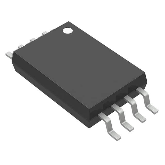
| Distributor | Stock | Pricing | MOQ | PKG | Lead Time | Date Code | On Order Quantity | On Order Delivery | |
|---|---|---|---|---|---|---|---|---|---|
|
231,795 pcs
|
231795 pcs | On Request | 1 | On Request | On Request | On Request | On Request | On Request | |
|
3,384 pcs
|
3384 pcs | On Request | 1 | On Request | On Request | 1822+ | On Request | On Request | |
|
2 pcs
|
2 pcs | On Request | 1 | On Request | On Request | On Request | On Request | On Request |
| Category | |
| Manufacturer Name | |
| Differential | |
| Frequency | |
| Input | |
| Input Type | |
| Mounting Type | |
| Number of Circuits | |
| Number of Outputs | |
| Operating Temperature | |
| Output | |
| Ratio | |
| Supplier Device Package | |
| Supplier Package | |
| Type | |
| Voltage |
The CDCV304PWRG4 from Texas Instruments is a high-performance, low-skew, general-purpose PCI-X compliant clock buffer. It is designed to distribute one input clock signal (CLKIN) to a bank of four outputs (1Y[0:3]). This buffer is suitable for PCI-X applications and operates from a single 3.3-V or 2.5-V supply.
Key electrical specifications include an operating frequency of up to 200 MHz, low output skew of less than 100 ps, and typical additive RMS jitter of 56 fs. The input and output types are LVTTL. The device features an output enable control that drives outputs low when OE is low.
Packaged in an 8-TSSOP, the CDCV304PWRG4 is characterized for operation over an industrial temperature range of -40°C to 85°C. This makes it suitable for automotive and industrial applications. The buffer is designed for surface mount mounting.
This clock buffer is a reliable component for clock distribution networks requiring precise timing and low jitter. Its PCI-X compliance ensures compatibility with relevant standards.
The CDCV304PWRG4 operates at a maximum frequency of 200 MHz.
The CDCV304PWRG4 provides 4 outputs.
The typical output skew for the CDCV304PWRG4 is less than 100 ps.
The CDCV304PWRG4 operates in a temperature range of -40°C to 85°C.
The CDCV304PWRG4 is supplied in an 8-TSSOP package.
The CDCV304PWRG4 supports core and output supply voltages of 2.5V and 3.3V.