

| Distributor | Stock | Pricing | MOQ | PKG | Lead Time | Date Code | On Order Quantity | On Order Delivery | |
|---|---|---|---|---|---|---|---|---|---|
|
1,000 pcs
|
1000 pcs | On Request | 1 | On Request | On Request | 08+ | On Request | On Request | |
|
340 pcs
|
340 pcs | On Request | 1 | On Request | On Request | 09+ | On Request | On Request |
| Category | |
| Manufacturer Name | |
| Differential | |
| Frequency | |
| Input | |
| Main Purpose | |
| Mounting Type | |
| Number of Circuits | |
| Operating Temperature | |
| Output | |
| PLL | |
| Ratio | |
| Supplier Device Package | |
| Tape & Reel | |
| Voltage |
The Texas Instruments CDCUA877ZQLR is an Application Specific Clock/Timing Integrated Circuit (IC) designed for Memory and DDR2 applications. This PLL clock driver features a maximum frequency of 410MHz and operates within a supply voltage range of 1.7V to 1.9V.
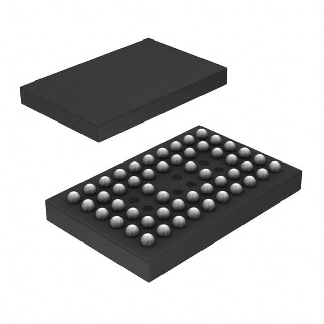
The device supports SSTL-18 input and output signaling with a 1:10 input to output ratio and differential signaling capabilities. It is housed in a 52-VFBGA package, specifically a 52-BGA MICROSTAR JUNIOR (7x4.5), and is designed for surface mount.
The operating temperature range for the CDCUA877ZQLR is -40°C to 85°C. It is specified as ROHS3 Compliant, with a Moisture Sensitivity Level (MSL) of 1 Unlimited, and REACH Unaffected status.
The operating voltage for the CDCUA877ZQLR is between 1.7V and 1.9V.
The CDCUA877ZQLR is available in a 52-VFBGA package.
The operating temperature range for the CDCUA877ZQLR is -40°C to 85°C.
The maximum frequency for the CDCUA877ZQLR is 410MHz.
The main purpose of the CDCUA877ZQLR is for Memory and DDR2 applications.