

| Distributor | Stock | Pricing | MOQ | PKG | Lead Time | Date Code | On Order Quantity | On Order Delivery | |
|---|---|---|---|---|---|---|---|---|---|
|
4,477 pcs
|
4477 pcs | On Request | 1 | On Request | On Request | 0636+ | On Request | On Request | |
|
2,320 pcs
|
2320 pcs | On Request | 1 | On Request | On Request | N/A | On Request | On Request |
| Category | |
| Manufacturer Name | |
| Differential | |
| Frequency | |
| Input | |
| Main Purpose | |
| Mounting Type | |
| Number of Circuits | |
| Operating Temperature | |
| Output | |
| PLL | |
| Ratio | |
| Supplier Device Package | |
| Voltage |
The Texas Instruments CDCU877ZQLR is a high-performance, low-jitter, low-skew clock driver. It is designed to distribute a single differential clock input to ten differential clock output pairs, making it suitable for Double Data Rate (DDR II) applications. The device operates at frequencies up to 400 MHz and features a low static phase offset of ±50 ps and low jitter of ±30 ps (cycle-to-cycle).
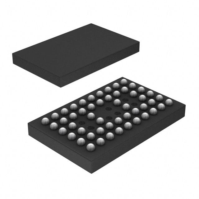
This clock driver supports SSTL-18 input and output standards and operates within a voltage range of 1.7V to 1.9V. The operating temperature range is -40°C to 85°C. The CDCU877ZQLR is available in a 52-ball MicroStar Junior BGA package, suitable for surface mounting.
Key features include a 1:10 input-to-output ratio, integrated PLL for synchronization, and compatibility with spread spectrum clocking for reduced EMI. The device also includes fail-safe inputs and a low current consumption of less than 135 mA. It meets or exceeds JESD82-8 PLL standards for PC2-3200/4300.
The CDCU877ZQLR is designed for applications requiring precise clock distribution and low noise. Its robust specifications make it a reliable choice for memory interfaces and other high-speed digital systems where clock integrity is critical.
The CDCU877ZQLR operates at frequencies up to 400 MHz.
The operating voltage for the CDCU877ZQLR is 1.7V to 1.9V.
The CDCU877ZQLR operates in a temperature range of -40°C to 85°C.
The CDCU877ZQLR is available in a 52-VFBGA package.
The main purpose of the CDCU877ZQLR is for Memory and DDR2 applications.
Yes, the CDCU877ZQLR features an integrated Phase Lock Loop (PLL).