

| Distributor | Stock | Pricing | MOQ | PKG | Lead Time | Date Code | On Order Quantity | On Order Delivery | |
|---|---|---|---|---|---|---|---|---|---|
|
22 pcs
|
22 pcs | On Request | 1 | On Request | On Request | 4 | On Request | On Request |
| Category | |
| Manufacturer Name | |
| AEC Qualified | |
| Automotive Grade | |
| Current Consumption | |
| Differential | |
| Frequency | |
| Industrial Grade | |
| Input | |
| Input Type | |
| Main Purpose | |
| Medical Grade | |
| Military Grade | |
| Mounting Type | |
| Number of Circuits | |
| Operating Temperature | |
| Output | |
| PLL | |
| Ratio | |
| Supplier Device Package | |
| Tape & Reel | |
| Voltage |
The CDCU877AGQLR from Texas Instruments is a high-performance, low-jitter, low-skew, zero-delay buffer designed for Double Data Rate (DDR II) applications. This device distributes a single differential clock input pair to ten differential clock output pairs and one differential feedback clock output pair.
Key electrical specifications include an operating frequency range of 10 MHz to 400 MHz and a low current consumption of less than 135 mA. It boasts low jitter with cycle-to-cycle jitter of ±30 ps, output skew of 35 ps, period jitter of ±20 ps, and dynamic phase offset of ±15 ps, with static phase offset at ±50 ps. The device operates from a voltage supply of 1.7V to 1.9V.
Designed for flexibility, the CDCU877AGQLR supports spread spectrum clocking for reduced EMI and features fail-safe inputs. It meets or exceeds the JESD82-8 PLL Standard for PC2-3200/4300. The device operates reliably within an ambient temperature range of -40°C to 85°C.
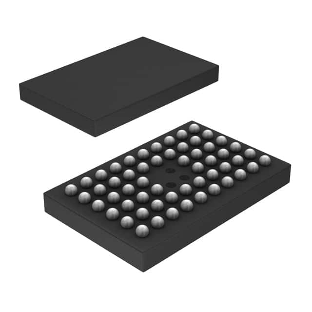
The CDCU877AGQLR is available in a 56-VFBGA package, suitable for surface mount applications. It is designed to synchronize outputs to input clocks using external feedback pins and supports both single-ended and differential input/output modes.
The operating voltage for the CDCU877AGQLR is 1.7V to 1.9V.
The maximum operating frequency of the CDCU877AGQLR is 400 MHz.
The CDCU877AGQLR is available in a 56-VFBGA package.
The operating temperature range for the CDCU877AGQLR is -40°C to 85°C.