

| Distributor | Stock | Pricing | MOQ | PKG | Lead Time | Date Code | On Order Quantity | On Order Delivery | |
|---|---|---|---|---|---|---|---|---|---|
|
45,200 pcs
|
45200 pcs | On Request | 1 | On Request | On Request | On Request | On Request | On Request | |
|
10,000 pcs
|
10000 pcs | On Request | 1 | On Request | On Request | 21+ | On Request | On Request | |
|
5,858 pcs
|
5858 pcs | On Request | 1 | On Request | On Request | 21 | On Request | On Request | |
|
1,468 pcs
|
1468 pcs | On Request | 1 | On Request | On Request | On Request | On Request | On Request |
| Category | |
| Manufacturer Name | |
| AEC Qualified | |
| Automotive Grade | |
| Differential | |
| Frequency | |
| Halogen Free | |
| Input | |
| Input Type | |
| Lead Style | |
| Mounting Type | |
| Number of Circuits | |
| Operating Temperature | |
| Output | |
| Ratio | |
| SVHC Present | |
| Supplier Device Package | |
| Tape & Reel | |
| Type | |
| Voltage |
The CDCS504TPWRQ1 from Texas Instruments is an automotive-qualified clock buffer and clock multiplier designed for versatile clock generation. It accepts a 3.3V LVCMOS input signal and utilizes a phased-locked loop (PLL) to either maintain the input frequency or multiply it by four, supporting output frequencies up to 108 MHz.
This device features selectable frequency multiplication with a single external control pin and an output enable/disable function controlled via a separate pin. It operates within a core and output supply voltage range of 3.3V and is characterized for an ambient operating temperature range of -40°C to 105°C.
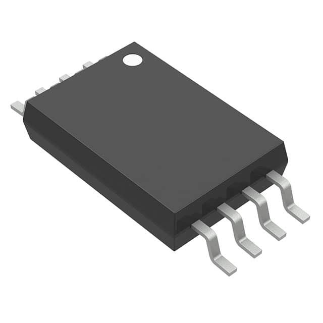
The CDCS504TPWRQ1 is housed in a compact 8-pin TSSOP package, making it suitable for space-constrained designs. Its pin programmability and wide temperature range make it a flexible solution for various timing applications in automotive environments.
Key specifications include LVCMOS input and output types, a maximum output frequency of 108 MHz, and a supply voltage range of 3V to 3.6V. The device is rated for Temperature Grade 2 and meets HBM ESD Classification Level H2 and CDM ESD Classification Level C3B.
| Qty | Low | High |
|---|---|---|
| 1+ | $0.76 | $0.76 |
Estimated market price range - modelled values for guidance only, not live distributor offers.
The maximum output frequency is 108 MHz.
The CDCS504TPWRQ1 uses LVCMOS input and LVCMOS output.
The device operates with a supply voltage between 3V and 3.6V.
The operating temperature range is -40°C to 105°C.
The CDCS504TPWRQ1 is supplied in an 8-TSSOP package.
Yes, the CDCS504TPWRQ1 is qualified for automotive applications.