

| Distributor | Stock | Pricing | MOQ | PKG | Lead Time | Date Code | On Order Quantity | On Order Delivery | |
|---|---|---|---|---|---|---|---|---|---|
|
51,657 pcs
|
51657 pcs | On Request | 1 | On Request | On Request | On Request | On Request | On Request | |
|
28,083 pcs
|
28083 pcs | On Request | 1 | On Request | On Request | On Request | On Request | On Request | |
|
3,056 pcs
|
3056 pcs | On Request | 1 | On Request | On Request | 14 | On Request | On Request | |
|
1,985 pcs
|
1985 pcs | On Request | 1 | On Request | On Request | On Request | On Request | On Request |
| Category | |
| Manufacturer Name | |
| Differential | |
| Frequency | |
| Input | |
| Mounting Type | |
| Number of Circuits | |
| Operating Temperature | |
| Output | |
| Ratio | |
| Supplier Device Package | |
| Tape & Reel | |
| Type | |
| Voltage |
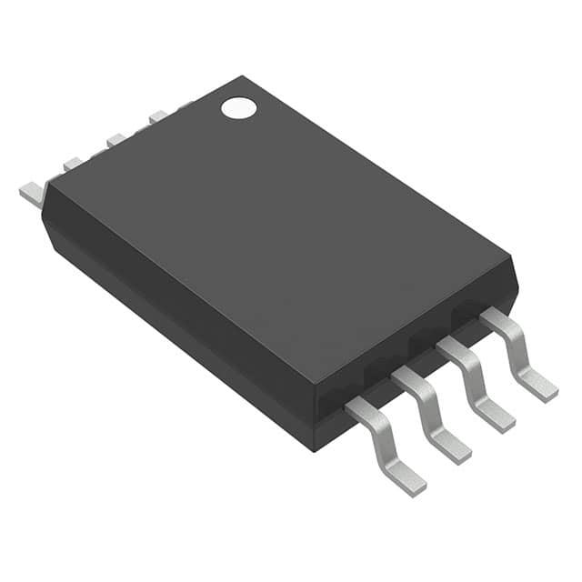
The CDCS503TPWRQ1 from Texas Instruments is an automotive-qualified clock buffer and clock multiplier designed for clock generation and distribution. This device features a selectable frequency multiplication factor of x1 or x4 and supports optional Spread Spectrum Clocking (SSC) with controllable modulation percentages.
With an LVCMOS input and output, the CDCS503TPWRQ1 operates from a 3.3V power supply and can generate output frequencies up to 108 MHz. It includes an output enable pin for control. The device is qualified for automotive applications under AEC-Q100, specifically meeting Device Temperature Grade 2 requirements, with an operating temperature range of -40°C to 105°C.
Packaged in an 8-pin TSSOP, the CDCS503TPWRQ1 is suitable for applications requiring low space consumption. Its robust design and automotive qualification make it a reliable choice for clock network synchronization in demanding environments.
Key specifications include a 3.3V operating voltage, a maximum frequency of 108 MHz, and an operating temperature range of -40°C to 105°C. The component is surface-mount and comes in an 8-TSSOP package with a standard reel quantity of 2,000 units.
| Qty | Low | High |
|---|---|---|
| 1+ | $0.77 | $0.77 |
Estimated market price range - modelled values for guidance only, not live distributor offers.
The CDCS503TPWRQ1 operates from a 3V to 3.6V supply.
The maximum frequency for the CDCS503TPWRQ1 is 108 MHz.
The operating temperature range is -40°C to 105°C.
The CDCS503TPWRQ1 is available in an 8-TSSOP package.
Yes, the CDCS503TPWRQ1 is RoHS3 Compliant.
The Moisture Sensitivity Level (MSL) is Level 1.
Yes, the CDCS503TPWRQ1 features optional Spread Spectrum Clocking (SSC).