

| Distributor | Stock | Pricing | MOQ | PKG | Lead Time | Date Code | On Order Quantity | On Order Delivery | |
|---|---|---|---|---|---|---|---|---|---|
|
58,093 pcs
|
58093 pcs | On Request | 1 | On Request | On Request | On Request | On Request | On Request | |
|
36,160 pcs
|
36160 pcs | On Request | 1 | On Request | On Request | On Request | On Request | On Request | |
|
35,690 pcs
|
35690 pcs | On Request | 1 | On Request | On Request | 21+ | On Request | On Request |
| Category | |
| Manufacturer Name | |
| Conflict Minerals | |
| Differential | |
| Frequency | |
| Halogen Free | |
| Input | |
| Input Type | |
| Lead Style | |
| Mounting Type | |
| Number of Circuits | |
| Operating Temperature | |
| Output | |
| Ratio | |
| SVHC Present | |
| Supplier Device Package | |
| Supplier Package | |
| Tape & Reel | |
| Type | |
| Voltage |
The CDCS503PWR from Texas Instruments is a versatile clock buffer and multiplier designed for consumer and industrial applications requiring EMI reduction. This device features an LVCMOS input and can multiply the input frequency by a factor of 1 or 4.
Key electrical specifications include a maximum output frequency of 108 MHz, a core and output supply voltage of 3.3V, and LVCMOS input and output types. The operating temperature range is -40°C to 85°C.
A notable feature is the optional Spread-Spectrum Clocking (SSC) capability, which can be controlled via two external pins. The SSC modulation offers center spread options of ±0%, ±0.5%, ±1%, or ±2%. Frequency multiplication is selectable between x1 or x4 using one external control pin. An output enable pin is also included for control.
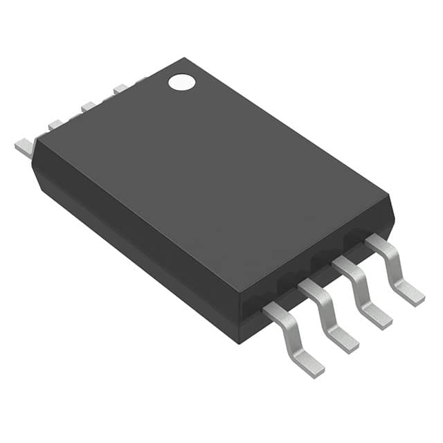
The CDCS503PWR is housed in a compact 8-TSSOP package, making it suitable for space-constrained designs. Its ability to reduce EMI through SSC and provide frequency multiplication makes it ideal for applications where clock signal integrity and electromagnetic compatibility are critical.
| Qty | Low | High |
|---|---|---|
| 1+ | $0.66 | $0.66 |
Estimated market price range - modelled values for guidance only, not live distributor offers.
The maximum output frequency is 108 MHz.
The CDCS503PWR operates on a single 3.3V power supply.
The CDCS503PWR uses LVCMOS for both input and output.
The operating temperature range is -40°C to 85°C.
Yes, the CDCS503PWR supports optional Spread-Spectrum Clocking (SSC) controllable via 2 external pins with modulation up to ±2% center spread.
The CDCS503PWR is available in an 8-TSSOP package.