

| Distributor | Stock | Pricing | MOQ | PKG | Lead Time | Date Code | On Order Quantity | On Order Delivery | |
|---|---|---|---|---|---|---|---|---|---|
|
5,590 pcs
|
5590 pcs | On Request | 1 | On Request | On Request | 1444+ | On Request | On Request |
| Category | |
| Manufacturer Name | |
| Differential | |
| Divider | |
| Features | |
| Frequency | |
| Input | |
| Input Type | |
| Lead Style | |
| Mounting Type | |
| Number of Circuits | |
| Number of Outputs | |
| Operating Temperature | |
| Operating Temperature Range | |
| Output | |
| Output Type | |
| PLL | |
| Ratio | |
| Supplier Device Package | |
| Supplier Package | |
| Type | |
| Voltage |
The CDCS501PWR from Texas Instruments is a spread spectrum capable, LVCMOS input clock buffer designed to mitigate EMI issues in electronic designs. It accepts a 3.3V LVCMOS signal and can spread this signal by a small amount, centered around the input frequency, with the spread amount selectable via control pins.
Key electrical specifications include a maximum output frequency of 108MHz, a core and output supply voltage of 3.3V, and LVCMOS input and output types. The device operates within a temperature range of -40°C to 85°C.
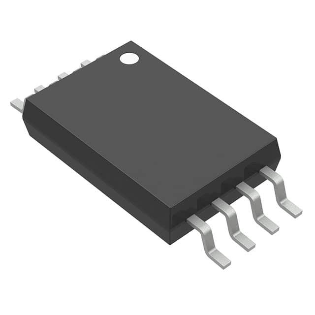
This clock driver is housed in an 8-pin TSSOP package, measuring 3 mm x 6.4 mm, making it suitable for applications requiring low space consumption. It is part of a family of easy-to-use clock generator devices with optional spread-spectrum clocking (SSC) capabilities, controllable via external pins.
Applications include consumer and industrial systems that require EMI reduction through spread spectrum clocking. The device is designed to counter common EMI problems in modern electronic designs.
| Qty | Low | High |
|---|---|---|
| 1+ | $0.55 | $0.55 |
Estimated market price range - modelled values for guidance only, not live distributor offers.
The maximum output frequency is 108MHz.
The CDCS501PWR uses LVCMOS for both input and output.
The operating voltage is 3.3V.
The operating temperature range is -40°C to 85°C.
The CDCS501PWR is supplied in an 8-TSSOP package.
Yes, the CDCS501PWR is a spread spectrum capable clock driver.