

| Distributor | Stock | Pricing | MOQ | PKG | Lead Time | Date Code | On Order Quantity | On Order Delivery | |
|---|---|---|---|---|---|---|---|---|---|
|
23,371 pcs
|
23371 pcs | On Request | 1 | On Request | On Request | On Request | On Request | On Request | |
|
5,810 pcs
|
5810 pcs | On Request | 1 | On Request | On Request | 0936+ | On Request | On Request |
| Category | |
| Manufacturer Name | |
| Differential | |
| Frequency | |
| Input | |
| Input Type | |
| Mounting Type | |
| Number of Circuits | |
| Number of Outputs | |
| Operating Temperature | |
| Output | |
| Ratio | |
| Supplier Device Package | |
| Type | |
| Voltage |
The CDCM1804RGER from Texas Instruments is a versatile clock buffer designed for efficient clock distribution. It takes a single differential clock input and distributes it to three LVPECL differential clock outputs and one LVCMOS single-ended output.
This device supports signaling rates up to 800 MHz for LVPECL and 200 MHz for LVCMOS. It features a programmable output divider for two LVPECL outputs and the LVCMOS output, offering flexibility in design. The CDCM1804RGER is optimized for driving 50-ohm transmission lines and minimizes noise during signal transitions with a 1.6 ns skew between LVCMOS and LVPECL outputs.
Key electrical characteristics include a core and output supply voltage range of 3V to 3.6V, additive RMS jitter of 150 fs (typical), and output skew of 30 ps for LVPECL outputs. The input stage accepts various differential and single-ended signaling types, including LVDS, HSTL, CML, VML, SSTL-2, and LVTTL/LVCMOS.
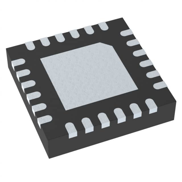
The CDCM1804RGER is housed in a 24-VQFN (4x4 mm) package, suitable for surface mount applications. It operates within a temperature range of -40°C to 85°C.
| Qty | Low | High |
|---|---|---|
| 1+ | $7.20 | $7.20 |
Estimated market price range - modelled values for guidance only, not live distributor offers.
The supply voltage range is 3V to 3.6V.
The CDCM1804RGER is available in a 24-VQFN Exposed Pad package.
The operating temperature range is -40°C to 85°C.
The RoHS status is RoHS3 Compliant.
The device supports up to 800 MHz for LVPECL signaling.
It has three LVPECL outputs and one LVCMOS output.