

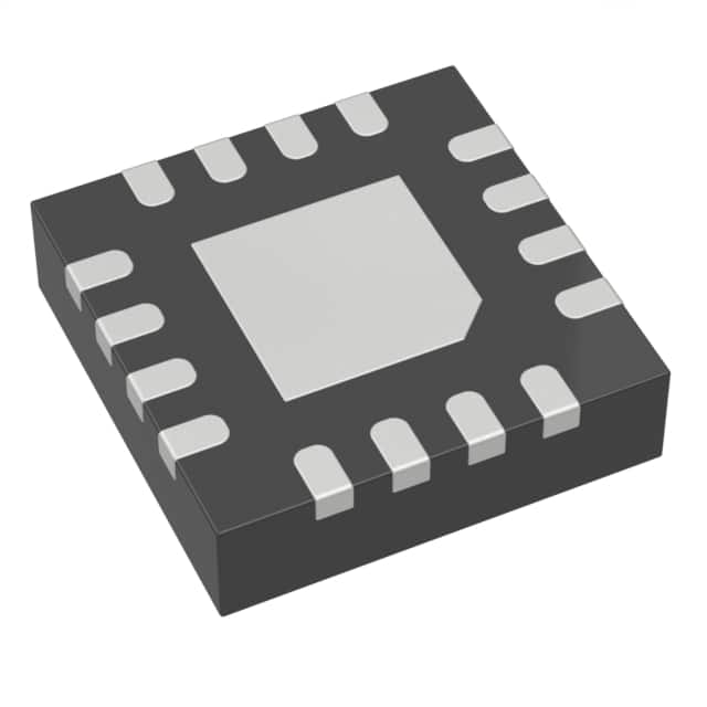
| Distributor | Stock | Pricing | MOQ | PKG | Lead Time | Date Code | On Order Quantity | On Order Delivery | |
|---|---|---|---|---|---|---|---|---|---|
|
6,696 pcs
|
6696 pcs | On Request | 1 | On Request | On Request | On Request | On Request | On Request | |
|
3,667 pcs
|
3667 pcs | On Request | 1 | On Request | On Request | On Request | On Request | On Request | |
|
1,075 pcs
|
1075 pcs | On Request | 1 | On Request | On Request | 13+ | On Request | On Request | |
|
140 pcs
|
140 pcs | On Request | 1 | On Request | On Request | On Request | On Request | On Request |
| Category | |
| Manufacturer Name | |
| Differential | |
| Frequency | |
| Input | |
| Input Type | |
| Mounting Type | |
| Number of Circuits | |
| Number of Outputs | |
| Operating Temperature | |
| Output | |
| Output Type | |
| Ratio | |
| Supplier Device Package | |
| Tape & Reel | |
| Type | |
| Voltage |
The CDCM1802RGTR from Texas Instruments is a versatile clock buffer designed to distribute one differential clock input to one LVPECL differential clock output pair and one single-ended LVCMOS output. It is engineered for driving 50-ohm transmission lines, ensuring signal integrity.
Key electrical specifications include a maximum signaling rate of 800 MHz for LVPECL and 200 MHz for LVCMOS outputs. The device operates with a core and output supply voltage of 3.3V, with 2.5V functional capability. It offers an additive RMS jitter of 150 fs (typical) and an output skew of 1600 ps between LVCMOS and LVPECL transitions, minimizing noise impact.
The CDCM1802RGTR features a programmable output divider for both LVPECL and LVCMOS outputs, controlled by two 3-level input pins (S0, S1). An enable pin (EN) allows for simultaneous disabling or enabling of all outputs. The device includes a differential input stage for a wide common-mode range and provides a VBB output for single-ended driver applications.
Packaged in a compact 16-pin VQFN (3mm x 3mm) with surface mount type, this clock buffer is characterized for operation in an industrial temperature range of -40°C to 85°C. Its design makes it suitable for applications requiring precise clock signal distribution and management.
| Qty | Low | High |
|---|---|---|
| 1+ | $6.31 | $6.31 |
Estimated market price range - modelled values for guidance only, not live distributor offers.
The CDCM1802RGTR operates from -40°C to 85°C.
The CDCM1802RGTR is available in a 16-VQFN (3x3) package.
The CDCM1802RGTR features LVCMOS and LVPECL output types.
The CDCM1802RGTR supports a maximum signaling rate of 800 MHz for LVPECL outputs.
The CDCM1802RGTR operates with a core and output supply voltage of 3.3V.
The typical additive RMS jitter for the CDCM1802RGTR is 150 fs.
The output skew between LVCMOS and LVPECL transitions is 1600 ps.