

| Distributor | Stock | Pricing | MOQ | PKG | Lead Time | Date Code | On Order Quantity | On Order Delivery | |
|---|---|---|---|---|---|---|---|---|---|
|
16,917 pcs
|
16917 pcs | On Request | 1 | On Request | On Request | On Request | On Request | On Request | |
|
364 pcs
|
364 pcs | On Request | 1 | On Request | On Request | On Request | On Request | On Request |
| Category | |
| Manufacturer Name | |
| Differential | |
| ESD Protection | |
| Frequency | |
| Input | |
| Mounting Type | |
| Number of Circuits | |
| Number of Outputs | |
| Operating Temperature | |
| Output | |
| Ratio | |
| Supplier Device Package | |
| Type | |
| Voltage |
The CDCLVP2106RHAT from Texas Instruments is a high-performance, low additive jitter clock buffer. It features dual 1:6 differential buffering, providing 12 LVPECL outputs from two universal clock inputs. These inputs can accept LVPECL, LVDS, or LVCMOS/LVTTL signals.
This device operates with a core and output supply voltage range of 2.375V to 3.6V and supports a maximum clock frequency of 2 GHz. It offers very low additive jitter, specified as less than 0.1 ps RMS in the 10-kHz to 20-MHz offset range. The maximum propagation delay is 550 ps, and the maximum within-bank output skew is 20 ps.
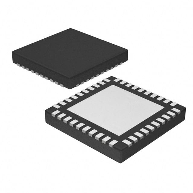
The CDCLVP2106RHAT is housed in a 40-pin VQFN package with dimensions of 6 mm x 6 mm. It is designed for surface mounting and operates within an industrial temperature range of -40°C to 85°C. ESD protection exceeds 2000 V (HBM).
This clock buffer is suitable for various communication applications requiring precise clock distribution with minimal jitter and skew.
| Qty | Low | High |
|---|---|---|
| 1+ | $9.12 | $9.12 |
Estimated market price range - modelled values for guidance only, not live distributor offers.
The maximum clock frequency supported is 2 GHz.
The CDCLVP2106RHAT provides 12 LVPECL outputs.
The operating temperature range is -40°C to 85°C.
The device operates with a supply voltage between 2.375V and 3.6V.
It is available in a 40-VQFN (6x6mm) package.
The maximum within-bank output skew is 20 ps.