

| Distributor | Stock | Pricing | MOQ | PKG | Lead Time | Date Code | On Order Quantity | On Order Delivery | |
|---|---|---|---|---|---|---|---|---|---|
|
4,018 pcs
|
4018 pcs | On Request | 1 | On Request | On Request | On Request | On Request | On Request | |
|
845 pcs
|
845 pcs | On Request | 1 | On Request | On Request | 17+ | On Request | On Request | |
|
122 pcs
|
122 pcs | On Request | 1 | On Request | On Request | 17+ | On Request | On Request | |
|
110 pcs
|
110 pcs | On Request | 1 | On Request | On Request | On Request | On Request | On Request |
| Category | |
| Manufacturer Name | |
| Differential | |
| ESD Protection | |
| Frequency | |
| Input | |
| Input Voltage | |
| Lead Style | |
| Mounting Type | |
| Number of Circuits | |
| Operating Temperature | |
| Operating Temperature Range | |
| Output | |
| Output Voltage | |
| Propagation Delay | |
| Ratio | |
| Supplier Device Package | |
| Supplier Package | |
| Type | |
| Voltage |
The CDCLVP2102RGTR from Texas Instruments is a versatile, low additive jitter clock buffer capable of generating four LVPECL clock outputs from two universal inputs. It supports LVPECL, LVDS, and LVCMOS/LVTTL input types, making it suitable for a wide range of communication applications.
This buffer operates at a maximum clock frequency of 2 GHz and offers a core supply voltage range of 2.5V to 3.3V. Key electrical characteristics include very low additive jitter of less than 100 fs RMS and a maximum propagation delay of 450 ps. The device also boasts a maximum within-bank output skew of 10 ps, ensuring precise clock signal distribution.
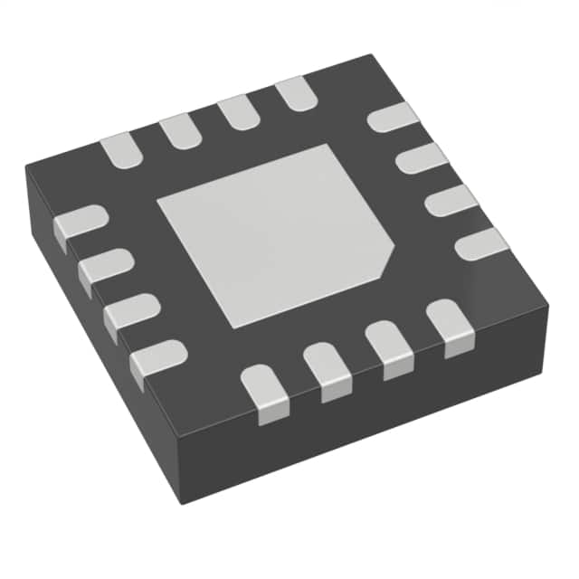
Packaged in a 16-VQFN (3x3 mm) surface-mount package, the CDCLVP2102RGTR is designed for efficient integration into compact electronic systems. It operates within an industrial temperature range of -40°C to 85°C and provides ESD protection exceeding 2000 V (HBM).
With its dual 1:2 differential buffer architecture, the CDCLVP2102RGTR is an excellent choice for demanding clock distribution tasks where signal integrity and low jitter are critical.
| Qty | Low | High |
|---|---|---|
| 1+ | $3.86 | $3.86 |
Estimated market price range - modelled values for guidance only, not live distributor offers.
The operating temperature range is -40°C to +85°C.
It is available in a 16-VQFN Exposed Pad package.
The maximum clock frequency is 2 GHz.
It supports LVCMOS, LVDS, LVPECL, and LVTTL input types.
The output type is LVPECL.
The device power supply range is 2.375V to 3.6V.
The additive RMS jitter is less than 100 fs.