

| Distributor | Stock | Pricing | MOQ | PKG | Lead Time | Date Code | On Order Quantity | On Order Delivery | |
|---|---|---|---|---|---|---|---|---|---|
|
55,381 pcs
|
55381 pcs | On Request | 1 | On Request | On Request | On Request | On Request | On Request | |
|
3,616 pcs
|
3616 pcs | On Request | 1 | On Request | On Request | On Request | On Request | On Request | |
|
3,466 pcs
|
3466 pcs | On Request | 1 | On Request | On Request | On Request | On Request | On Request |
| Category | |
| Manufacturer Name | |
| Differential | |
| ESD Protection | |
| Frequency | |
| Input | |
| Mounting Type | |
| Number of Circuits | |
| Number of Outputs | |
| Operating Temperature | |
| Operating Voltage | |
| Output | |
| Ratio | |
| Supplier Device Package | |
| Supplier Package | |
| Type | |
| Voltage |
The Texas Instruments CDCLVP1216RGZT is a high-performance clock buffer designed for communication applications. It features a 2:16 fanout ratio, capable of generating 16 LVPECL clock outputs from one of two selectable universal inputs (LVPECL, LVDS, or LVCMOS).
This buffer supports a maximum clock frequency of 2 GHz and boasts very low additive jitter, typically 57 fs RMS at 122.88 MHz. The output skew is minimized to 30 ps, ensuring signal integrity. The device operates over an industrial temperature range of -40°C to 85°C and is powered by a core supply voltage of 2.5V or 3.3V, with output voltages also at 2.5V or 3.3V.
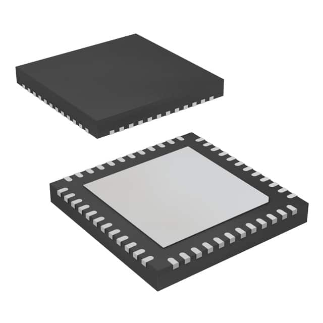
The CDCLVP1216RGZT is housed in a compact 48-VQFN (7x7 mm) package with an exposed pad for enhanced thermal performance. It features selectable clock inputs via a control pin and ESD protection exceeding 2000V (HBM). Its low jitter and high frequency capabilities make it suitable for demanding timing applications.
| Qty | Low | High |
|---|---|---|
| 1+ | $12.93 | $12.93 |
Estimated market price range - modelled values for guidance only, not live distributor offers.
The maximum clock frequency is 2 GHz.
It supports LVCMOS, LVDS, LVPECL, and LVTTL input types.
The CDCLVP1216RGZT has 16 outputs.
The typical additive RMS jitter at 122.88 MHz is 57 fs.
The operating temperature range is -40°C to 85°C.
It is available in a 48-VQFN (7x7mm) package.