

| Distributor | Stock | Pricing | MOQ | PKG | Lead Time | Date Code | On Order Quantity | On Order Delivery | |
|---|---|---|---|---|---|---|---|---|---|
|
5,281 pcs
|
5281 pcs | On Request | 1 | On Request | On Request | 1601+ | On Request | On Request | |
|
3,747 pcs
|
3747 pcs | On Request | 1 | On Request | On Request | On Request | On Request | On Request | |
|
3,480 pcs
|
3480 pcs | On Request | 1 | On Request | On Request | On Request | On Request | On Request | |
|
882 pcs
|
882 pcs | On Request | 1 | On Request | On Request | 20+ | On Request | On Request | |
|
46 pcs
|
46 pcs | On Request | 1 | On Request | On Request | On Request | On Request | On Request | |
|
2 pcs
|
2 pcs | On Request | 1 | On Request | On Request | On Request | On Request | On Request |
| Category | |
| Manufacturer Name | |
| B0 | |
| Differential | |
| ESD Protection | |
| Frequency | |
| Input | |
| Input Type | |
| Mounting Type | |
| Number of Circuits | |
| Number of Outputs | |
| Operating Temperature | |
| Output | |
| Output Type | |
| Ratio | |
| Supplier Device Package | |
| Type | |
| Voltage | |
| w |
The CDCLVP1204RGTR from Texas Instruments is a versatile, low additive jitter clock buffer designed to generate four LVPECL clock outputs from selectable LVPECL, LVDS, or LVCMOS inputs. This device is suitable for various communication applications requiring high-performance clock distribution.
Key electrical specifications include a maximum clock frequency of 2 GHz, a core supply voltage range of 2.375V to 3.6V, and a maximum propagation delay of 450 ps. The buffer boasts very low additive jitter, typically 57 fs RMS at 122.88 MHz, and minimal output skew as low as 15 ps. It accepts universal inputs including LVCMOS, LVDS, and LVPECL, and provides four LVPECL outputs.
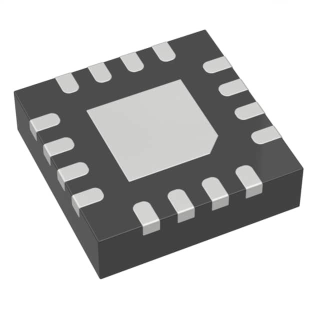
This clock buffer operates within an industrial temperature range of -40°C to 85°C. It is housed in a 16-VQFN (3x3 mm) package, suitable for surface mount applications. The device features an on-chip multiplexer for input selection, configurable via a control terminal.
With its low jitter, low skew, and high frequency capabilities, the CDCLVP1204RGTR is an excellent choice for demanding clock tree designs in communication systems and other high-speed applications.
| Qty | Low | High |
|---|---|---|
| 1+ | $1.53 | $1.53 |
Estimated market price range - modelled values for guidance only, not live distributor offers.
The maximum clock frequency is 2 GHz.
It supports LVCMOS, LVDS, and LVPECL input types.
The output type is LVPECL.
The operating temperature range is -40°C to 85°C.
It is a 16-VQFN Exposed Pad package suitable for surface mounting.
It provides 4 outputs.
The typical additive RMS jitter is 57 fs in the 10-kHz to 20-MHz offset range.