

| Distributor | Stock | Pricing | MOQ | PKG | Lead Time | Date Code | On Order Quantity | On Order Delivery | |
|---|---|---|---|---|---|---|---|---|---|
|
4,000 pcs
|
4000 pcs | On Request | 1 | On Request | On Request | 24+ | On Request | On Request | |
|
1,842 pcs
|
1842 pcs | On Request | 1 | On Request | On Request | On Request | On Request | On Request | |
|
402 pcs
|
402 pcs | On Request | 1 | On Request | On Request | 20+ | On Request | On Request | |
|
199 pcs
|
199 pcs | On Request | 1 | On Request | On Request | On Request | On Request | On Request | |
|
7 pcs
|
7 pcs | On Request | 1 | On Request | On Request | On Request | On Request | On Request | |
|
4 pcs
|
4 pcs | On Request | 1 | On Request | On Request | On Request | On Request | On Request |
| Category | |
| Manufacturer Name | |
| Clock Frequency | |
| Differential | |
| ESD Protection | |
| Frequency | |
| Input | |
| Input Type | |
| Mounting Type | |
| Number of Circuits | |
| Number of Outputs | |
| Operating Temperature | |
| Output | |
| Output Type | |
| Ratio | |
| Supplier Device Package | |
| Supplier Package | |
| Type | |
| Voltage |
The CDCLVD1208RHDT from Texas Instruments is a 2:8 differential clock buffer capable of distributing one of two selectable clock inputs to eight LVDS outputs. This device supports universal inputs, accepting LVDS, LVPECL, and LVCMOS signals, making it versatile for various clocking applications.
Key electrical specifications include a maximum clock frequency of 800 MHz, low additive RMS jitter of typically 171 fs (10 kHz to 20 MHz), and a maximum output skew of 45 ps. The device operates with a core and output supply voltage of 2.5 V, with a device power supply range of 2.375 V to 2.625 V. It also features ESD protection exceeding 3-kV HBM and 1-kV CDM.
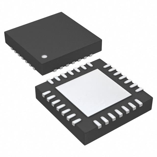
The CDCLVD1208RHDT is packaged in a 28-pin VQFN (5x5 mm) with an exposed pad, suitable for surface mounting. Its industrial operating temperature range is -40°C to 85°C. Applications include telecommunications, networking, medical imaging, test and measurement equipment, and wireless communications.
This buffer is designed for driving 50-ohm transmission lines. For single-ended input operation, an appropriate bias voltage (V AC_REF) must be applied to the unused negative input pin. The input selection is managed via a control pin (IN_SEL).
| Qty | Low | High |
|---|---|---|
| 1+ | $6.01 | $6.01 |
Estimated market price range - modelled values for guidance only, not live distributor offers.
The output type is LVDS.
The operating temperature range is -40°C to 85°C.
It is supplied in a 28-VQFN (5x5) package.
The RoHS status is RoHS3 Compliant.
The device supports a clock frequency of up to 800 MHz.
It accepts LVCMOS, LVDS, and LVPECL input types.
The typical additive RMS jitter is 171 fs in the 10-kHz to 20-MHz range.