

| Distributor | Stock | Pricing | MOQ | PKG | Lead Time | Date Code | On Order Quantity | On Order Delivery | |
|---|---|---|---|---|---|---|---|---|---|
|
9,522 pcs
|
9522 pcs | On Request | 1 | On Request | On Request | 20+ | On Request | On Request | |
|
3,667 pcs
|
3667 pcs | On Request | 1 | On Request | On Request | On Request | On Request | On Request |
| Category | |
| Manufacturer Name | |
| Clock Frequency | |
| Differential | |
| Frequency | |
| Input | |
| Input Type | |
| Mounting Type | |
| Number of Circuits | |
| Number of Outputs | |
| Operating Temperature | |
| Output | |
| Output Type | |
| Ratio | |
| Supplier Device Package | |
| Supplier Package | |
| Type | |
| Voltage |
The CDCLVD1204RGTR from Texas Instruments is a 2:4 differential clock buffer designed for high-speed clock distribution. It accepts universal inputs including LVDS, LVPECL, and LVCMOS, allowing for flexible signal interfacing.
This device offers low additive jitter, specified at less than 300fs RMS in the 10kHz to 20MHz range, and a low output skew of 20ps maximum. It supports clock frequencies up to 800MHz and operates from a core and output supply voltage of 2.5V, with a range of 2.375V to 2.625V.
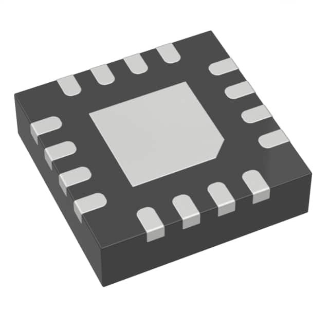
The CDCLVD1204RGTR is suitable for driving 50-ohm transmission lines and features selectable clock inputs via a control pin. It is packaged in a compact 16-pin VQFN (3mm x 3mm) with an exposed pad, designed for surface mounting.
With an operating temperature range of -40°C to 85°C, this clock buffer is well-suited for industrial applications requiring reliable clock signal integrity.
| Qty | Low | High |
|---|---|---|
| 1+ | $3.67 | $3.67 |
Estimated market price range - modelled values for guidance only, not live distributor offers.
The operating temperature range is -40°C to 85°C.
The CDCLVD1204RGTR supports LVCMOS, LVDS, and LVPECL inputs.
The maximum clock frequency is 800 MHz.
The CDCLVD1204RGTR is supplied in a 16-VQFN (3x3mm) package.
The output skew is a maximum of 20 ps.
The additive RMS jitter is less than 300 fs RMS in the 10kHz to 20MHz range.