

| Distributor | Stock | Pricing | MOQ | PKG | Lead Time | Date Code | On Order Quantity | On Order Delivery | |
|---|---|---|---|---|---|---|---|---|---|
|
5,740 pcs
|
5740 pcs | On Request | 1 | On Request | On Request | On Request | On Request | On Request | |
|
2,260 pcs
|
2260 pcs | On Request | 1 | On Request | On Request | 09+ | On Request | On Request | |
|
2,200 pcs
|
2200 pcs | On Request | 1 | On Request | On Request | 24+ | On Request | On Request |
| Category | |
| Manufacturer Name | |
| Differential | |
| Frequency | |
| Halogen Free | |
| Input | |
| Input Type | |
| Mounting Type | |
| Number of Circuits | |
| Number of Outputs | |
| Operating Temperature | |
| Output | |
| Output Type | |
| Ratio | |
| SVHC Present | |
| Supplier Device Package | |
| Tape & Reel | |
| Type | |
| Voltage |
The Texas Instruments CDCLVD110AVF is a high-performance clock buffer designed to distribute a single differential LVDS clock input to ten LVDS differential clock outputs. This device is optimized for clock distribution applications, offering a typical signaling rate capability of up to 1.1 GHz and low output skew of less than 30 ps. The CDCLVD110AVF operates with a core and output supply voltage range of 2.375V to 2.625V, centered around 2.5V.
Key electrical characteristics include an additive RMS jitter of 111 fs (typical) and a receiver input threshold of ±100 mV. The device features a configurable register for individually enabling or disabling outputs and selecting between CLK0 or CLK1 inputs. It is designed to drive 50-ohm transmission lines and includes fail-safe I/O pins for power-down conditions.
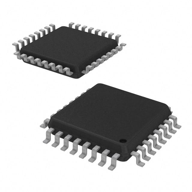
Packaged in a 32-pin LQFP (7x7 mm), the CDCLVD110AVF is suitable for surface mount applications. It operates within an ambient temperature range of -40°C to 85°C, making it robust for various environmental conditions. This clock buffer is ideal for applications requiring precise clock signal distribution with minimal skew.
| Qty | Low | High |
|---|---|---|
| 1+ | $8.28 | $8.28 |
Estimated market price range - modelled values for guidance only, not live distributor offers.
The operating temperature range is -40°C to 85°C.
The CDCLVD110AVF is available in a 32-LQFP package.
The CDCLVD110AVF supports a frequency of 1.1 GHz.
The typical output skew is 50 ps.
The core and output supply voltage is 2.5V.