

| Distributor | Stock | Pricing | MOQ | PKG | Lead Time | Date Code | On Order Quantity | On Order Delivery | |
|---|---|---|---|---|---|---|---|---|---|
|
14,452 pcs
|
14452 pcs | On Request | 1 | On Request | On Request | On Request | On Request | On Request | |
|
1,436 pcs
|
1436 pcs | On Request | 1 | On Request | On Request | 1812+ | On Request | On Request | |
|
364 pcs
|
364 pcs | On Request | 1 | On Request | On Request | On Request | On Request | On Request |
| Category | |
| Manufacturer Name | |
| Differential | |
| Frequency | |
| Input | |
| Input Type | |
| Mounting Type | |
| Number of Circuits | |
| Number of Outputs | |
| Operating Temperature | |
| Output | |
| Output Type | |
| Ratio | |
| Supplier Device Package | |
| Supplier Package | |
| Type | |
| Voltage |
The CDCLVD110ARHBR from Texas Instruments is a high-performance clock buffer designed to distribute a single differential LVDS clock input to ten LVDS differential clock outputs. This device is optimized for clock distribution applications, offering a typical signaling rate capability of up to 1.1 GHz and a low output skew of 50 ps. It operates with a core and output supply voltage range of 2.375V to 2.625V, centered around 2.5V.
The CDCLVD110ARHBR features a configurable register for individually enabling or disabling outputs, providing flexibility in clock signal management. It supports both AC- and DC-coupled systems with an improved start-up circuit. The device is characterized for operation over an industrial temperature range of -40°C to 85°C.
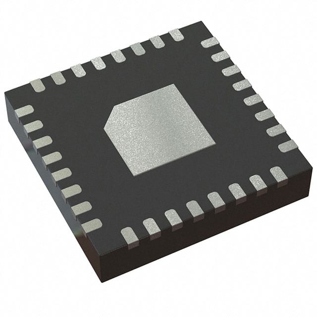
Packaged in a 32-pin VQFN (5x5 mm) with an exposed pad, the CDCLVD110ARHBR is suitable for surface mount applications. Its design focuses on minimizing skew for critical clock distribution networks in various electronic systems.
| Qty | Low | High |
|---|---|---|
| 1+ | $6.90 | $6.90 |
Estimated market price range - modelled values for guidance only, not live distributor offers.
The core and output supply voltage is 2.5V.
It is supplied in a 32-VFQFN exposed pad package.
The operating temperature range is -40°C to 85°C.
The typical additive RMS jitter is 111 fs.
It has a typical signaling rate capability of 1.1 GHz.
Both the input and output types are LVDS.
The typical output skew is less than 30 ps.