

| Distributor | Stock | Pricing | MOQ | PKG | Lead Time | Date Code | On Order Quantity | On Order Delivery | |
|---|---|---|---|---|---|---|---|---|---|
|
20,000 pcs
|
20000 pcs | On Request | 1 | On Request | On Request | On Request | On Request | On Request | |
|
9,043 pcs
|
9043 pcs | On Request | 1 | On Request | On Request | 17+ | On Request | On Request | |
|
3,235 pcs
|
3235 pcs | On Request | 1 | On Request | On Request | On Request | On Request | On Request | |
|
1,047 pcs
|
1047 pcs | On Request | 1 | On Request | On Request | On Request | On Request | On Request | |
|
542 pcs
|
542 pcs | On Request | 1 | On Request | On Request | 20+ | On Request | On Request | |
|
34 pcs
|
34 pcs | On Request | 1 | On Request | On Request | On Request | On Request | On Request | |
|
1 pcs
|
1 pcs | On Request | 1 | On Request | On Request | On Request | On Request | On Request |
| Category | |
| Manufacturer Name | |
| Differential | |
| Frequency | |
| Input | |
| Lead Spacing | |
| Mounting Type | |
| Number of Circuits | |
| Operating Temperature | |
| Output | |
| Ratio | |
| Supplier Device Package | |
| Tape & Reel | |
| Type | |
| Voltage |
The CDCLVC1108PWR from Texas Instruments is a modular, high-performance, low-skew, general-purpose clock buffer designed for LVCMOS clock generation. This device offers a 1:8 fan-out ratio, making it suitable for distributing clock signals across a system.
Key electrical characteristics include a very low pin-to-pin skew of less than 50 ps and very low additive jitter of less than 100 fs. It supports a supply voltage range of 2.3V to 3.6V. The maximum operating frequency is 250 MHz when operating at 3.3V, and 180 MHz at 2.5V. The buffer is designed for LVCMOS input and output signals.
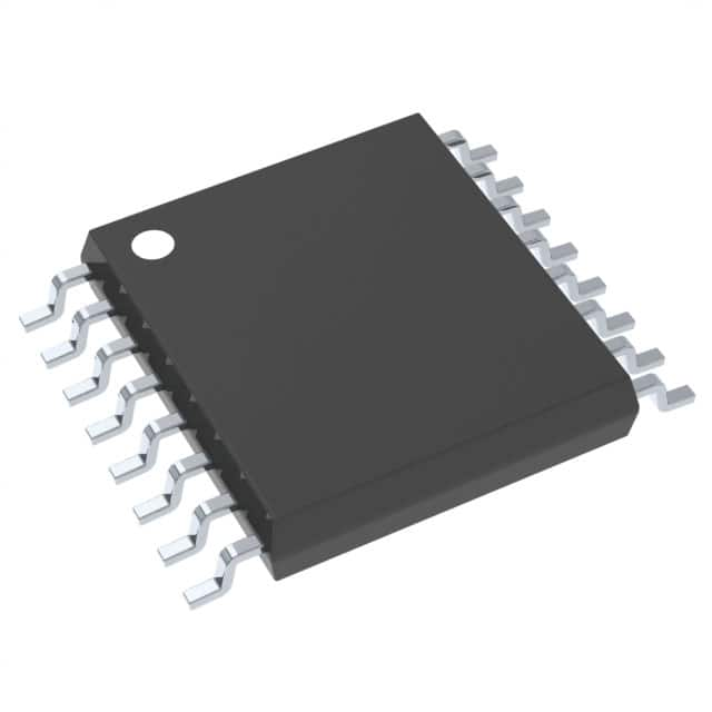
This clock buffer operates within a wide temperature range of -40°C to 85°C, ensuring reliable performance in various environmental conditions. It is housed in a compact 16-TSSOP package with a surface mount type, suitable for space-constrained applications. The CDCLVC11xx family, including the CDCLVC1108PWR, is designed for easy integration and pin compatibility among devices.
The CDCLVC11xx family supports an asynchronous output enable control which can switch outputs to a low state when the enable signal is low. This feature can be useful for power management or system reset sequences.
| Qty | Low | High |
|---|---|---|
| 1+ | $2.20 | $2.20 |
Estimated market price range - modelled values for guidance only, not live distributor offers.
The maximum operating frequency is 250 MHz at 3.3V and 180 MHz at 2.5V.
The operating voltage range is 2.3V to 3.6V.
The operating temperature range is -40°C to 85°C.
The CDCLVC1108PWR is supplied in a 16-TSSOP package.
The fan-out ratio is 1:8.
Yes, it features very low pin-to-pin skew of less than 50 ps.
The MSL rating is Level-1 Unlimited.