

| Distributor | Stock | Pricing | MOQ | PKG | Lead Time | Date Code | On Order Quantity | On Order Delivery | |
|---|---|---|---|---|---|---|---|---|---|
|
15,067 pcs
|
15067 pcs | On Request | 1 | On Request | On Request | On Request | On Request | On Request | |
|
185 pcs
|
185 pcs | On Request | 1 | On Request | On Request | On Request | On Request | On Request |
| Category | |
| Manufacturer Name | |
| Differential | |
| Frequency | |
| Input | |
| Input Type | |
| Mounting Type | |
| Number of Circuits | |
| Number of Outputs | |
| Operating Temperature | |
| Output | |
| Output Type | |
| Ratio | |
| Supplier Device Package | |
| Supplier Package | |
| Type | |
| Voltage |
The Texas Instruments CDCLVC1108PW is a high-performance, low-skew, general-purpose clock buffer designed for clock distribution applications. This device features a 1:8 fan-out ratio, supporting LVCMOS input and output types.
Key electrical characteristics include a maximum frequency of 250 MHz and very low additive RMS jitter of typically 70 fs. The output skew is minimal at 50 ps. The device operates with a core and output supply voltage range of 2.3 V to 3.6 V, and is specified for a wide operating temperature range of -40°C to 85°C.
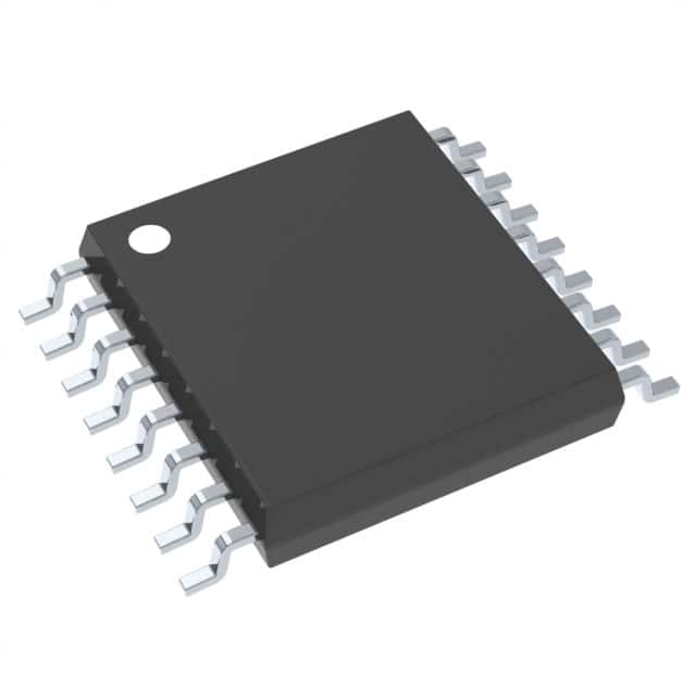
Packaged in a 16-TSSOP, the CDCLVC1108PW is designed for surface mount applications. Its modular design and pin-compatibility within the CDCLVC11xx family allow for easy integration into various clock generation systems. An asynchronous output enable control is also provided.
This clock buffer is suitable for applications requiring reliable clock signal distribution with minimal jitter and skew, such as in telecommunications, computing, and industrial systems.
| Qty | Low | High |
|---|---|---|
| 1+ | $2.64 | $2.64 |
Estimated market price range - modelled values for guidance only, not live distributor offers.
The CDCLVC1108PW has a 1:8 fan-out ratio.
The CDCLVC1108PW supports a maximum frequency of 250 MHz.
The typical additive RMS jitter for the CDCLVC1108PW is 70 fs.
The output skew for the CDCLVC1108PW is 50 ps.
The operating voltage range for the CDCLVC1108PW is 2.3 V to 3.6 V.
The CDCLVC1108PW operates from -40°C to 85°C.
The CDCLVC1108PW is available in a 16-TSSOP package.