

| Distributor | Stock | Pricing | MOQ | PKG | Lead Time | Date Code | On Order Quantity | On Order Delivery | |
|---|---|---|---|---|---|---|---|---|---|
|
45,200 pcs
|
45200 pcs | On Request | 1 | On Request | On Request | On Request | On Request | On Request | |
|
2,608 pcs
|
2608 pcs | On Request | 1 | On Request | On Request | 1440+ | On Request | On Request | |
|
1,635 pcs
|
1635 pcs | On Request | 1 | On Request | On Request | 15+ | On Request | On Request | |
|
1,119 pcs
|
1119 pcs | On Request | 1 | On Request | On Request | On Request | On Request | On Request | |
| On Request | On Request | 1 | On Request | On Request | On Request | On Request | On Request |
| Category | |
| Manufacturer Name | |
| Differential | |
| Frequency | |
| Halogen Free | |
| Input | |
| Input Type | |
| Lead Spacing | |
| Lead Style | |
| Mounting Type | |
| Number of Circuits | |
| Number of Outputs | |
| Operating Temperature | |
| Output | |
| Output Type | |
| Ratio | |
| Supplier Device Package | |
| Supplier Package | |
| Tape & Reel | |
| Type | |
| Voltage |
The Texas Instruments CDCLVC1104PW is a high-performance, low-skew, general-purpose LVCMOS clock buffer. It features a 1:4 fan-out ratio and operates at frequencies up to 250 MHz. The device supports core and output supply voltages of 2.5V and 3.3V, with an overall operating voltage range of 2.3V to 3.6V.
Designed for reliable clock distribution, the CDCLVC1104PW offers very low additive jitter of typically 70 fs and an output skew of 50 ps. It is suitable for applications requiring precise timing signals. The buffer operates within an industrial temperature range of -40°C to 85°C.
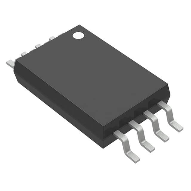
This clock buffer is available in an 8-TSSOP surface-mount package, measuring 3 mm x 6.4 mm. Its LVCMOS input and output types make it compatible with standard logic levels. The CDCLVC11xx family, to which this part belongs, is designed with a modular approach for easy integration into clock generation systems.
| Qty | Low | High |
|---|---|---|
| 1+ | $2.44 | $2.44 |
Estimated market price range - modelled values for guidance only, not live distributor offers.
The CDCLVC1104PW has a 1:4 fan-out ratio.
The maximum frequency for the CDCLVC1104PW is 250 MHz.
The typical additive RMS jitter for the CDCLVC1104PW is 70 fs.
The output skew of the CDCLVC1104PW is 50 ps.
The CDCLVC1104PW operates in a temperature range of -40°C to 85°C.
The CDCLVC1104PW supports core and output supply voltages of 2.5V and 3.3V, with an overall operating voltage range of 2.3V to 3.6V.
The CDCLVC1104PW is supplied in an 8-TSSOP package.