

| Distributor | Stock | Pricing | MOQ | PKG | Lead Time | Date Code | On Order Quantity | On Order Delivery | |
|---|---|---|---|---|---|---|---|---|---|
|
6,347 pcs
|
6347 pcs | On Request | 1 | On Request | On Request | 19+ | On Request | On Request | |
|
2,000 pcs
|
2000 pcs | On Request | 1 | On Request | On Request | On Request | On Request | On Request | |
|
1,623 pcs
|
1623 pcs | On Request | 1 | On Request | On Request | On Request | On Request | On Request | |
|
426 pcs
|
426 pcs | On Request | 1 | On Request | On Request | 20+ | On Request | On Request | |
|
3 pcs
|
3 pcs | On Request | 1 | On Request | On Request | On Request | On Request | On Request | |
|
3 pcs
|
3 pcs | On Request | 1 | On Request | On Request | On Request | On Request | On Request |
| Category | |
| Manufacturer Name | |
| Differential | |
| Frequency | |
| Input | |
| Input Type | |
| Mounting Type | |
| Number of Circuits | |
| Number of Outputs | |
| Operating Temperature | |
| Output | |
| Output Type | |
| Ratio | |
| Supplier Device Package | |
| Supplier Package | |
| Type | |
| Voltage |
The CDCLVC1103PWR is a 1:3 fan-out clock buffer from Texas Instruments, designed for high-performance clock distribution. It supports core and output supply voltages of 2.5V and 3.3V, making it versatile for various system requirements.
This buffer offers a maximum frequency of 250 MHz at 3.3V and 180 MHz at 2.5V. It boasts very low additive RMS jitter of typically 70 fs and low output skew of 50 ps, ensuring signal integrity. The device operates within a temperature range of -40°C to 85°C.
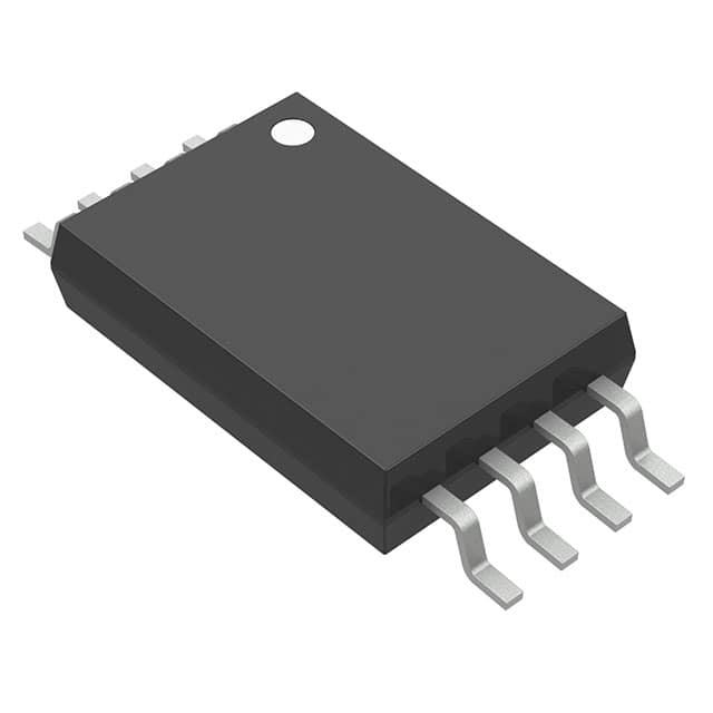
Packaged in an 8-TSSOP, the CDCLVC1103PWR is suitable for surface mount applications. Its input and output types are both LVCMOS, making it compatible with standard logic levels. The family of CDCLVC11xx devices is designed for modularity and pin-compatibility, simplifying design and board layout.
| Qty | Low | High |
|---|---|---|
| 1+ | $1.41 | $1.41 |
Estimated market price range - modelled values for guidance only, not live distributor offers.
The CDCLVC1103PWR has 3 outputs.
The typical additive RMS jitter is 70 fs.
It supports core and output supply voltages of 2.5V and 3.3V.
The maximum frequency is 250 MHz at 3.3V and 180 MHz at 2.5V.
The operating temperature range is -40°C to 85°C.
It is supplied in an 8-TSSOP package.
It is designed for surface mount.