

| Distributor | Stock | Pricing | MOQ | PKG | Lead Time | Date Code | On Order Quantity | On Order Delivery | |
|---|---|---|---|---|---|---|---|---|---|
|
1,975 pcs
|
1975 pcs | On Request | 1 | On Request | On Request | N/A | On Request | On Request |
| Category | |
| Manufacturer Name | |
| Differential | |
| Divider | |
| Frequency | |
| Halogen Free | |
| Input | |
| Lead Style | |
| Mounting Type | |
| Number of Circuits | |
| Operating Temperature | |
| Output | |
| PLL | |
| Ratio | |
| Supplier Device Package | |
| Supplier Package | |
| Type | |
| Voltage |
The CDCF5801DBQR from Texas Instruments is a low-jitter PLL-based multiplier and divider designed for clock generation applications. It supports an input frequency range of 12.5 MHz to 240 MHz and an output frequency range of 25 MHz to 280 MHz.
This device features programmable bidirectional delay steps down to 1.3 mUI, allowing for precise phase alignment. It accepts HSTL, LVPECL, and LVTTL input signals and can drive HSTL, LVDS, LVPECL, LVTTL, and SSTL outputs. The operating voltage range is 3V to 3.6V, with low power consumption of less than 190 mW at 280 MHz/3.3 V.
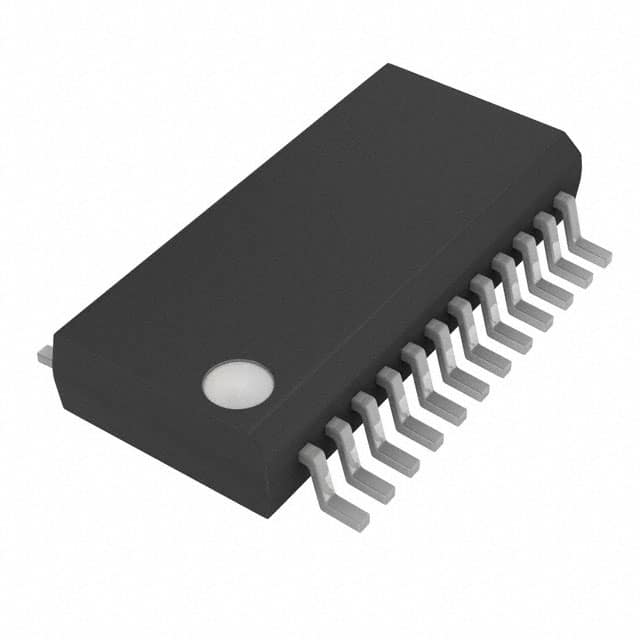
The CDCF5801DBQR is packaged in a 24-SSOP (0.154", 3.90mm Width) and is designed for surface mount applications. It operates within an ambient temperature range of -40°C to 85°C. This part is not recommended for new designs.
Applications for this clock multiplier include video graphics, gaming products, datacom, telecom, and noise cancellation created by FPGAs.
| Qty | Low | High |
|---|---|---|
| 1+ | $6.19 | $6.19 |
Estimated market price range - modelled values for guidance only, not live distributor offers.
The operating voltage is 3V ~ 3.6V.
The CDCF5801DBQR is available in a 24-SSOP package.
The operating temperature range is -40°C to 85°C.
The CDCF5801DBQR is RoHS3 Compliant.
The MSL is 1 Unlimited.
The maximum output frequency is 280 MHz.
It supports HSTL, LVPECL, and LVTTL input signals.