

| Distributor | Stock | Pricing | MOQ | PKG | Lead Time | Date Code | On Order Quantity | On Order Delivery | |
|---|---|---|---|---|---|---|---|---|---|
|
498 pcs
|
498 pcs | On Request | 1 | On Request | On Request | 17+ | On Request | On Request |
| Category | |
| Manufacturer Name | |
| Differential | |
| Frequency | |
| Input | |
| Lead Spacing | |
| Lead Style | |
| Main Purpose | |
| Mounting Type | |
| Number of Circuits | |
| Operating Temperature | |
| Operating Voltage | |
| Output | |
| PLL | |
| Ratio | |
| Supplier Device Package | |
| Tape & Reel | |
| Voltage |
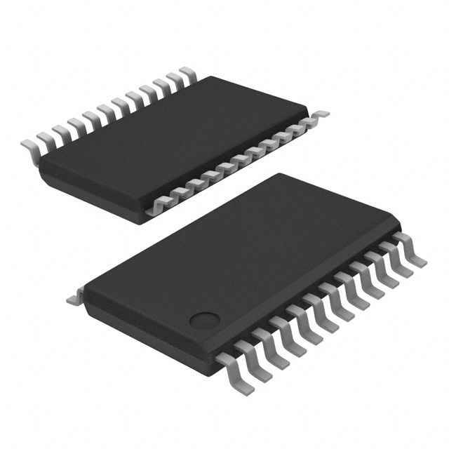
The Texas Instruments CDCF2510PW is a high-performance, low-skew, low-jitter phase-lock loop (PLL) clock driver. It operates at 3.3V and is designed to meet PC133 SDRAM Registered DIMM specifications.
This device distributes one clock input to one bank of 10 outputs, providing low-skew, low-jitter copies of the input clock. The output duty cycles are adjusted to 50%, independent of the input clock duty cycle. An output enable pin allows for enabling or disabling all 10 outputs.
The CDCF2510PW features on-chip series damping resistors, eliminating the need for external RC networks. It is available in a 24-TSSOP package and operates over a temperature range of 0°C to 85°C. Its main purpose is for Memory and DRAM DIMM applications.
Key electrical characteristics include an operating frequency range of 25 MHz to 140 MHz, static phase error distribution of ±125 ps at 66 MHz to 133 MHz, and jitter (cyc-cyc) of |70| ps at 66 MHz to 133 MHz. The device is designed to be compatible with spread spectrum clocking.
The operating voltage is 3.3V.
The operating temperature range is 0°C to 85°C.
The CDCF2510PW is available in a 24-TSSOP package.
The maximum operating frequency is 140 MHz.
The static phase error distribution is a maximum of ±125 ps.
The cycle-to-cycle jitter is |70| ps.
The main purpose is for Memory, DRAM DIMM.