

| Distributor | Stock | Pricing | MOQ | PKG | Lead Time | Date Code | On Order Quantity | On Order Delivery | |
|---|---|---|---|---|---|---|---|---|---|
|
11,800 pcs
|
11800 pcs | On Request | 1 | On Request | On Request | 0314+ | On Request | On Request |
| Category | |
| Manufacturer Name | |
| Differential | |
| Frequency | |
| Halogen Free | |
| Input | |
| Lead Style | |
| Main Purpose | |
| Mounting Type | |
| Number of Circuits | |
| Operating Temperature | |
| Output | |
| PLL | |
| Ratio | |
| Supplier Device Package | |
| Supplier Package | |
| Voltage |
The CDCF2509PWR from Texas Instruments is a high-performance, low-skew, low-jitter PLL clock driver. It operates at 3.3V and is specifically designed for synchronous DRAM applications, supporting the PC133 SDRAM Registered DIMM specification.
This device distributes one clock input to one bank of five outputs and another bank of four outputs, providing a total of nine clock copies. Each output bank can be enabled or disabled separately. The PLL precisely aligns the feedback output to the clock input in both frequency and phase. Integrated series-damping resistors are included, making it suitable for driving point-to-point loads.
The CDCF2509PWR features an operating frequency range of 25 MHz to 140 MHz. It offers a static phase error distribution of ±125 ps and cycle-to-cycle jitter of ±70 ps at 66 MHz to 133 MHz. The output signal duty cycles are adjusted to 50%, independent of the input clock duty cycle.
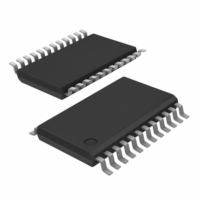
Packaged in a 24-TSSOP, the CDCF2509PWR is designed for surface mounting. It operates within a temperature range of 0°C to 70°C. Note that this part is not recommended for new designs, and the CDCVF2509A is suggested as an alternate.
| Qty | Low | High |
|---|---|---|
| 1+ | $11.67 | $11.67 |
Estimated market price range - modelled values for guidance only, not live distributor offers.
The CDCF2509PWR operates at 3.3V.
The CDCF2509PWR is available in a 24-TSSOP package.
The operating temperature range is 0°C to 70°C.
The CDCF2509PWR is RoHS3 Compliant.
The CDCF2509PWR has an operating frequency of up to 140 MHz.
The CDCF2509PWR provides 9 outputs.
No, the CDCF2509PWR is not recommended for new designs.