

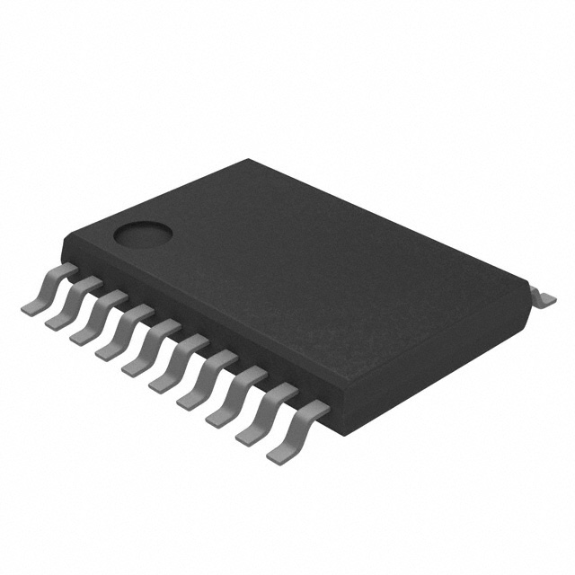
| Distributor | Stock | Pricing | MOQ | PKG | Lead Time | Date Code | On Order Quantity | On Order Delivery | |
|---|---|---|---|---|---|---|---|---|---|
|
5,040 pcs
|
5040 pcs | On Request | 1 | On Request | On Request | On Request | On Request | On Request | |
|
507 pcs
|
507 pcs | On Request | 1 | On Request | On Request | On Request | On Request | On Request | |
|
325 pcs
|
325 pcs | On Request | 1 | On Request | On Request | On Request | On Request | On Request | |
|
99 pcs
|
99 pcs | On Request | 1 | On Request | On Request | 1006 | On Request | On Request |
| Category | |
| Manufacturer Name | |
| Differential | |
| Divider | |
| Features | |
| Frequency | |
| Input | |
| Input Type | |
| Mounting Type | |
| Number of Circuits | |
| Number of Outputs | |
| Operating Temperature | |
| Output | |
| Output Type | |
| PLL | |
| Ratio | |
| Supplier Device Package | |
| Type | |
| Voltage |
The CDCE906PW from Texas Instruments is a high-performance, 3:6 PLL-based clock synthesizer, multiplier, and divider. This device is designed for generating precise video and audio system clocks from multiple sampling frequencies. It accepts crystal frequencies from 8 MHz up to 54 MHz, and LVCMOS or differential input frequencies up to 167 MHz.
Key features include user-programmable PLL frequencies with EEPROM programming, easy in-circuit programming via SMBus data interface, and a wide PLL divider ratio for 0-ppm output clock error. The CDCE906PW provides six LVCMOS outputs, each with a programmable output switching matrix and a 7-bit post-divider. It also incorporates spread-spectrum clocking (SSC) for lowering system EMI, with programmable center spread and down spread modulation options. Programmable output slew-rate control (SRC) is also available.
This clock synthesizer operates from a 3.3V power supply and is rated for a commercial temperature range of 0°C to 70°C. It is supplied in a 20-pin TSSOP package, suitable for surface mounting. The device includes features like I2C interface and integrated EEPROM for configuration.
Development and programming are facilitated by the TI Pro-Clock™ kit, simplifying PLL design and programming.
| Qty | Low | High |
|---|---|---|
| 1+ | $3.07 | $3.07 |
Estimated market price range - modelled values for guidance only, not live distributor offers.
The maximum output frequency for the CDCE906PW is 167MHz.
The CDCE906PW has 6 LVCMOS outputs.
The CDCE906PW operates on a core and output supply voltage of 3.3V.
The operating temperature range for the CDCE906PW is 0°C to 70°C.
The CDCE906PW is supplied in a 20-TSSOP package.
Yes, the CDCE906PW features programmable spread-spectrum clocking (SSC) for lowering system EMI.
The CDCE906PW accepts differential, LVCMOS, and crystal input signals.