

| Distributor | Stock | Pricing | MOQ | PKG | Lead Time | Date Code | On Order Quantity | On Order Delivery | |
|---|---|---|---|---|---|---|---|---|---|
|
129,203 pcs
|
129203 pcs | On Request | 1 | On Request | On Request | On Request | On Request | On Request | |
|
750 pcs
|
750 pcs | On Request | 1 | On Request | On Request | 21+ | On Request | On Request |
| Category | |
| Manufacturer Name | |
| Differential | |
| Frequency | |
| Halogen Free | |
| Input | |
| Input Type | |
| Lead Style | |
| Mounting Type | |
| Number of Circuits | |
| Operating Temperature | |
| Output | |
| Power Consumption | |
| Ratio | |
| Supplier Device Package | |
| Tape & Reel | |
| Type | |
| Voltage |
The Texas Instruments CDCDB2000NPPT is a 20-output fanout buffer designed for clock distribution in high-speed systems. It supports interfaces such as PCIe Gen 1-7, QPI, UPI, SAS, and SATA.
Key electrical specifications include a maximum frequency of 250 MHz, an operating voltage range of 3.135V to 3.465V, and low additive phase jitter of less than 0.08ps rms. The buffer offers 20 LP-HCSL outputs with integrated terminations and features 8 hardware output enable controls for individual output management.
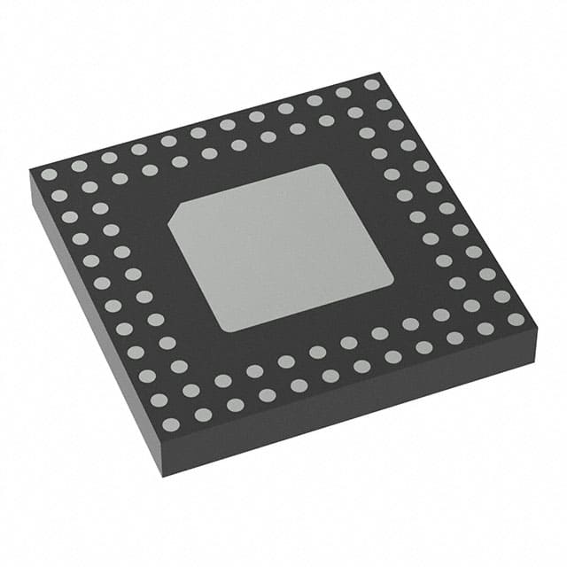
This device is packaged in an 80-lead TLGA/GQFN package measuring 6mm x 6mm and is designed for surface mount applications. The operating temperature range is -40°C to 85°C. It also supports hardware-controlled low power mode and has 9 selectable SMBus addresses for configuration.
The CDCDB2000NPPT meets or exceeds system parameters specified in the DB2000QL specification, making it suitable for demanding clocking applications.
| Qty | Low | High |
|---|---|---|
| 1+ | $3.66 | $3.66 |
Estimated market price range - modelled values for guidance only, not live distributor offers.
The operating voltage range is 3.135V to 3.465V.
The CDCDB2000NPPT is available in an 80-TLGA (6x6) package.
The operating temperature range is -40°C to 85°C.
The RoHS status is Compliant.
The output ratio is 1:20.
The maximum frequency is 250MHz.
The additive phase jitter is less than 0.08 ps rms.