


| Distributor | Stock | Pricing | MOQ | PKG | Lead Time | Date Code | On Order Quantity | On Order Delivery | |
|---|---|---|---|---|---|---|---|---|---|
|
2,016 pcs
|
2016 pcs | On Request | 1 | On Request | On Request | 24+ | On Request | On Request |
| Category | |
| Manufacturer Name | |
| Differential | |
| Divider | |
| Frequency | |
| Input | |
| Mounting Type | |
| Number of Circuits | |
| Operating Temperature | |
| Output | |
| PLL | |
| Ratio | |
| Supplier Device Package | |
| Type | |
| Voltage |
The Texas Instruments CDC857-2DGG is a high-performance, low-skew, low-jitter phase-lock loop (PLL) clock driver. It operates with a supply voltage range of 2.3V to 2.7V and can achieve a maximum frequency of 167MHz.
This device distributes one differential clock input to ten differential outputs, with a ratio of 1:10. It supports LVTTL and SSTL-2 input types and SSTL-2 output types. The operating temperature range is from 0°C to 85°C.
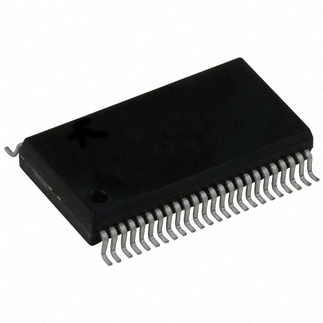
The CDC857-2DGG is packaged in a 48-TSSOP (Thin Shrink Small-Outline Package) and is designed for surface mounting. It features on-chip loop filtering, eliminating the need for external RC networks, which minimizes component count and board space.
Key features include spread spectrum clocking tracking capability to reduce EMI and adjustable output duty cycles to 50%, independent of the input duty cycle. An output enable input allows all outputs to be enabled or disabled.
The operating voltage for the CDC857-2DGG is between 2.3V and 2.7V.
The operating temperature range is 0°C to 85°C.
The CDC857-2DGG is available in a 48-TSSOP package, suitable for surface mounting.
Yes, the CDC857-2DGG is RoHS3 Compliant.
The maximum frequency is 167MHz.
It supports LVTTL and SSTL-2 input signal types and SSTL-2 output signal types.
Yes, it has a PLL with a bypass option for test purposes.