

| Distributor | Stock | Pricing | MOQ | PKG | Lead Time | Date Code | On Order Quantity | On Order Delivery | |
|---|---|---|---|---|---|---|---|---|---|
|
144 pcs
|
144 pcs | On Request | 1 | On Request | On Request | On Request | On Request | On Request |
| Category | |
| Manufacturer Name | |
| Differential | |
| Divider | |
| Frequency | |
| Input | |
| Mount | |
| Mounting Type | |
| Number of Circuits | |
| Number of Elements | |
| Number of Inputs | |
| Number of Outputs | |
| Operating Temperature | |
| Output | |
| PLL | |
| Ratio | |
| Supplier Device Package | |
| Type | |
| Voltage |
The Texas Instruments CDC7005ZVA is a single LVCMOS clock buffer, functioning as a clock synchronizer and jitter cleaner. It supports a maximum operating frequency of 800MHz and is designed to operate within a supply voltage range of 3V to 3.6V, with a typical operating voltage of 3.3V.
This component is suitable for applications requiring precise clock signal management. It features both LVCMOS and LVPECL inputs and LVPECL outputs, with a ratio of 2:5 and a divider function. The device operates across a wide temperature range from -40°C to 85°C.
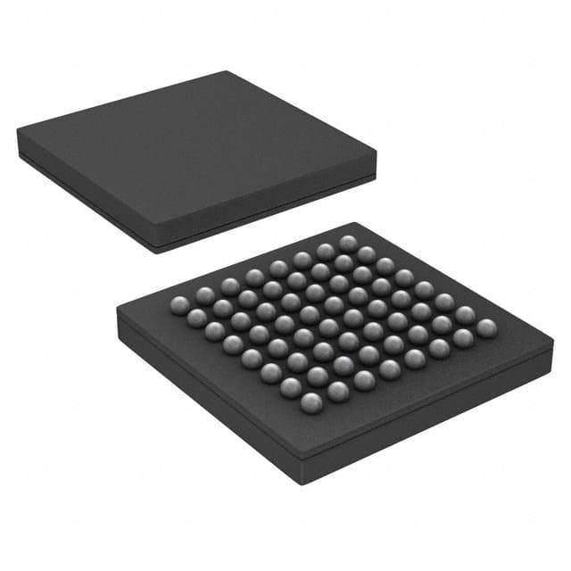
The CDC7005ZVA is packaged in a 64-LFBGA (8x8) format, designed for surface mount applications. It is RoHS3 compliant and lead-free, making it suitable for modern electronic assemblies. The device is part of the CDC7005 series.
Key specifications include its 800MHz maximum frequency, 3.3V operating voltage, and -40°C to 85°C operating temperature range. The 64-LFBGA package and surface mount capability are important considerations for board layout and assembly.
The maximum operating frequency is 800MHz.
It supports LVCMOS and LVPECL inputs and LVPECL outputs.
The operating supply voltage is 3.3V, with a range of 3V to 3.6V.
The operating temperature range is -40°C to 85°C.
It is available in a 64-BGA (8x8) package for surface mounting.
No, the CDC7005ZVA does not have a PLL.
The frequency ratio is 2:5.