

| Distributor | Stock | Pricing | MOQ | PKG | Lead Time | Date Code | On Order Quantity | On Order Delivery | |
|---|---|---|---|---|---|---|---|---|---|
|
11,950 pcs
|
11950 pcs | On Request | 1 | On Request | On Request | On Request | On Request | On Request | |
|
834 pcs
|
834 pcs | On Request | 1 | On Request | On Request | On Request | On Request | On Request |
| Category | |
| Manufacturer Name | |
| Differential | |
| Divider | |
| Frequency | |
| Input | |
| Input Type | |
| Mounting Type | |
| Number of Circuits | |
| Number of Outputs | |
| Operating Temperature | |
| Output | |
| PLL | |
| Ratio | |
| Supplier Device Package | |
| Type | |
| Voltage |
The Texas Instruments CDC516DGGR is a high-performance, low-skew, low-jitter, phase-lock loop (PLL) clock driver. It operates at a 3.3V core and output supply voltage, distributing one clock input to sixteen LVTTL outputs. The device is designed for synchronous DRAM applications and features separate output enable for each of the four banks of four outputs.
Key electrical specifications include an additive RMS jitter of 200 fs (typical), an output skew of 200 ps (typical), and a maximum frequency of 125 MHz. The operating temperature range is 0°C to 70°C. The CDC516 includes an on-chip loop filter, eliminating the need for external RC networks, which minimizes component count and board space.
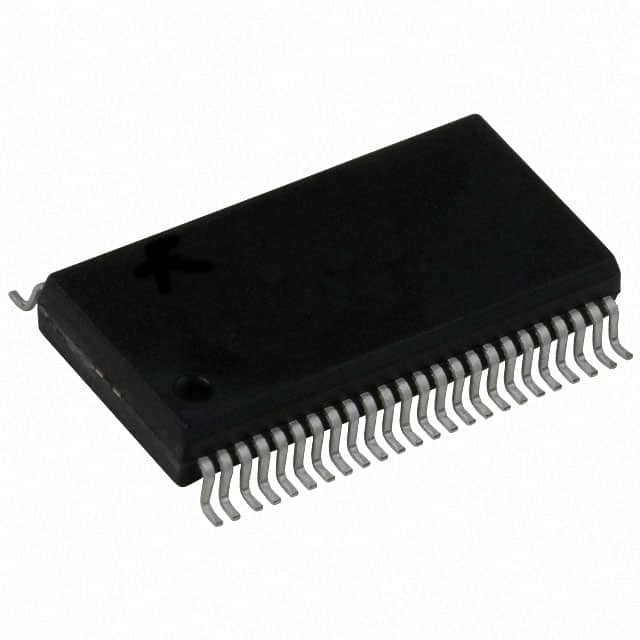
Packaged in a 48-TSSOP, the CDC516DGGR is suitable for surface mount applications. The device offers a 1:16 ratio and supports a 3V to 3.6V input voltage range. Its PLL can be bypassed for testing purposes. The output signal duty cycles are adjusted to 50 percent, independent of the input clock duty cycle.
The core supply voltage is 3.3V.
The operating temperature range is 0°C to 70°C.
The CDC516DGGR has 16 outputs.
The CDC516DGGR is supplied in a 48-TSSOP package.
The typical output skew is 200 ps.
Yes, the CDC516DGGR features a PLL with bypass capability.