

| Distributor | Stock | Pricing | MOQ | PKG | Lead Time | Date Code | On Order Quantity | On Order Delivery | |
|---|---|---|---|---|---|---|---|---|---|
|
6,987 pcs
|
6987 pcs | On Request | 1 | On Request | On Request | 06+ | On Request | On Request | |
|
6,060 pcs
|
6060 pcs | On Request | 1 | On Request | On Request | On Request | On Request | On Request | |
|
4,916 pcs
|
4916 pcs | On Request | 1 | On Request | On Request | 0040+ | On Request | On Request |
| Category | |
| Manufacturer Name | |
| Differential | |
| Divider | |
| Frequency | |
| Input | |
| Input Type | |
| Mounting Type | |
| Number of Circuits | |
| Number of Outputs | |
| Operating Temperature | |
| Operating Temperature Range | |
| Output | |
| Output Type | |
| PLL | |
| Ratio | |
| Supplier Device Package | |
| Supplier Package | |
| Type | |
| Voltage |
The Texas Instruments CDC509PWR is a high-performance, low-skew, low-jitter, phase-lock loop (PLL) clock driver. It precisely aligns the feedback output to the clock input signal in both frequency and phase, making it ideal for synchronous DRAM applications.
This device operates at a 3.3V core and output supply voltage and can drive up to nine clock loads. It features one bank of five outputs and another bank of four outputs, providing nine low-skew, low-jitter copies of the input clock. The output signal duty cycles are adjusted to 50 percent, independent of the input clock's duty cycle. Each output bank can be enabled or disabled separately using control inputs.
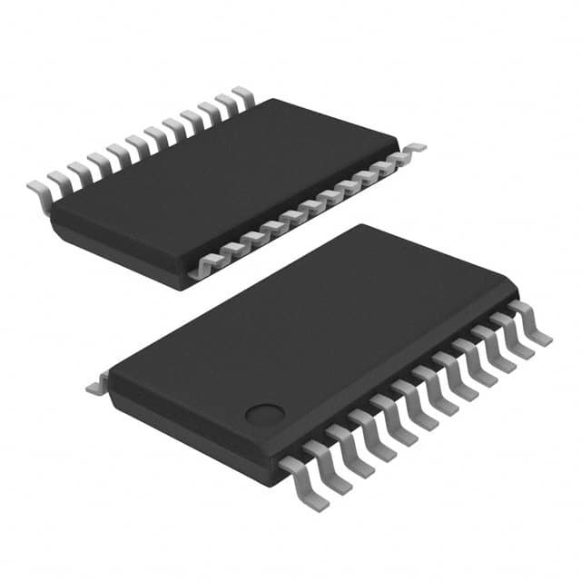
The CDC509PWR does not require external RC networks as the PLL loop filter is integrated on-chip, reducing component count and board space. It is packaged in a 24-pin Thin Shrink Small-Outline Package (TSSOP) with a surface mount type. The operating temperature range is from 0°C to 70°C.
Key electrical specifications include a frequency of 125MHz, an output skew of 200 ps, and an additive RMS jitter of 200 fs. The input and output signal types are LVTTL.
The operating voltage for the CDC509PWR is 3V to 3.6V.
The CDC509PWR is available in a 24-TSSOP package.
The operating temperature range for the CDC509PWR is 0°C to 70°C.
The CDC509PWR is RoHS3 Compliant.
The CDC509PWR has 9 outputs.
The output skew of the CDC509PWR is 200 ps.
The frequency of the CDC509PWR is 125MHz.