

| Distributor | Stock | Pricing | MOQ | PKG | Lead Time | Date Code | On Order Quantity | On Order Delivery | |
|---|---|---|---|---|---|---|---|---|---|
|
23,481 pcs
|
23481 pcs | On Request | 1 | On Request | On Request | On Request | On Request | On Request |
| Category | |
| Manufacturer Name | |
| Input Type | |
| Mounting Type | |
| Number of Outputs | |
| Output Type |
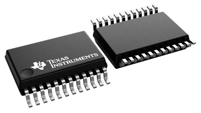
The Texas Instruments CDC351DBG4 is a high-performance clock driver designed for clock distribution and generation applications. It distributes a single clock input to ten outputs with minimal skew, making it suitable for precise timing requirements.
This device operates at a nominal 3.3-V core supply voltage and features LVTTL-compatible inputs and outputs. It supports mixed-mode signal operation, allowing 5-V input and output voltages with a 3.3-V core supply. The CDC351DBG4 offers low output skew of 0.6 ps and low pulse skew, ensuring signal integrity.
Key electrical characteristics include high-drive outputs capable of -32-mA I OH and 32-mA I OL. The device operates within a temperature range of -40°C to 85°C. It is available in SSOP (DB) and SOIC (DW) packages, both surface-mount types.
The output-enable (OE) pin allows the outputs to be disabled to a high-impedance state. Propagation delays are adjusted at the factory to minimize part-to-part skew. Pins P0 and P1 are intended for factory adjustment and should be connected to GND by the user.
| Qty | Low | High |
|---|---|---|
| 1+ | $11.07 | $11.07 |
Estimated market price range - modelled values for guidance only, not live distributor offers.
The core supply voltage for the CDC351DBG4 is 3.3 V.
The CDC351DBG4 has 10 outputs.
The output skew of the CDC351DBG4 is 0.6 ps.
The operating temperature range for the CDC351DBG4 is -40°C to 85°C.
The CDC351DBG4 features LVTTL-compatible inputs and outputs.
The CDC351DBG4 is available in SSOP (DB) and SOIC (DW) packages.