

| Distributor | Stock | Pricing | MOQ | PKG | Lead Time | Date Code | On Order Quantity | On Order Delivery | |
|---|---|---|---|---|---|---|---|---|---|
|
7,631 pcs
|
7631 pcs | On Request | 1 | On Request | On Request | On Request | On Request | On Request | |
|
3,200 pcs
|
3200 pcs | On Request | 1 | On Request | On Request | 0406+ | On Request | On Request |
| Category | |
| Manufacturer Name | |
| Differential | |
| Divider | |
| Frequency | |
| Input | |
| Input Type | |
| Lead Style | |
| Mounting Type | |
| Number of Circuits | |
| Number of Outputs | |
| Operating Temperature | |
| Operating Voltage | |
| Output | |
| Output Type | |
| PLL | |
| Ratio | |
| Supplier Device Package | |
| Supplier Package | |
| Tape & Reel | |
| Type | |
| Voltage |
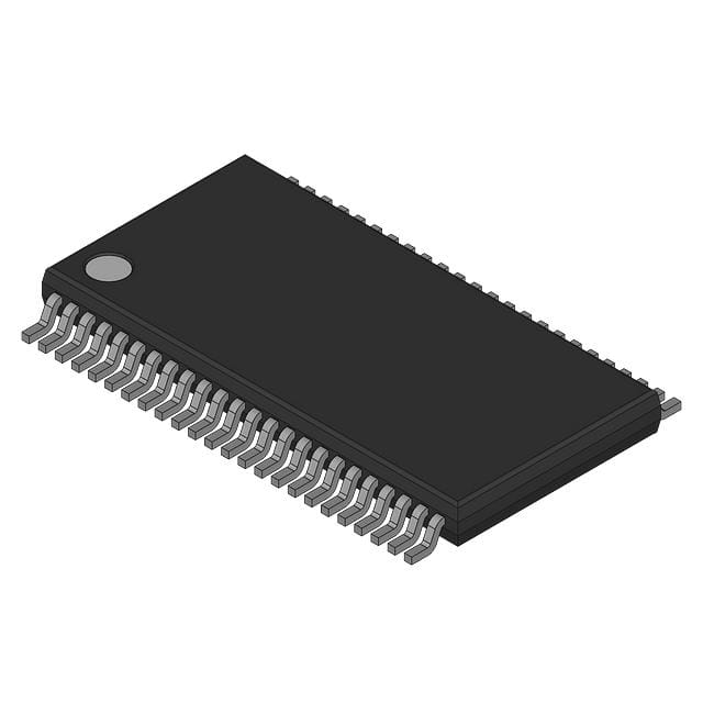
The Texas Instruments CDC2516DGGR is a high-performance, low-skew, low-jitter, phase-lock loop (PLL) clock driver. It precisely aligns the feedback output to the clock input signal, making it ideal for synchronous DRAM applications.
This device operates at a 3.3V core and output supply voltage, distributing one clock input to 16 low-skew, low-jitter copies across four banks of four outputs. Each bank can be enabled or disabled independently. The CDC2516 features on-chip series-damping resistors and an integrated loop filter, eliminating the need for external RC networks.
It has a frequency of 125MHz, an output skew of 250ps, and additive RMS jitter of 200fs (typ). The operating temperature range is 0°C to 70°C. The CDC2516DGGR is packaged in a 48-TSSOP surface-mount package.
Designed for ease of use and minimal component count, this PLL clock driver simplifies board design and reduces costs. It requires a stabilization time after power-up or signal application to achieve phase lock.
| Qty | Low | High |
|---|---|---|
| 1+ | $6.14 | $6.14 |
Estimated market price range - modelled values for guidance only, not live distributor offers.
The core supply voltage is 3.3V.
The output supply voltage is 3.3V.
The operating temperature range is 0°C to 70°C.
The CDC2516DGGR has 16 outputs.
It is a PLL Clock Driver.
The output skew is 250ps.
The typical additive RMS jitter is 200fs.