

| Distributor | Stock | Pricing | MOQ | PKG | Lead Time | Date Code | On Order Quantity | On Order Delivery | |
|---|---|---|---|---|---|---|---|---|---|
|
9,435 pcs
|
9435 pcs | On Request | 1 | On Request | On Request | 10+ | On Request | On Request | |
|
172 pcs
|
172 pcs | On Request | 1 | On Request | On Request | 0544+ | On Request | On Request |
| Category | |
| Manufacturer Name | |
| Differential | |
| Divider | |
| Frequency | |
| Input | |
| Mounting Type | |
| Number of Circuits | |
| Number of Outputs | |
| Operating Temperature | |
| Output | |
| PLL | |
| Power Dissipation | |
| Quiescent Current | |
| Ratio | |
| Supplier Device Package | |
| Supply Current | |
| Type | |
| Voltage |
The Texas Instruments CDC2510BPWR is a high-performance, low-skew, low-jitter phase-lock loop (PLL) clock driver. It operates at 3.3V and is designed to meet PC SDRAM Registered DIMM specifications. The device distributes one clock input to one bank of ten outputs, ensuring precise alignment in both frequency and phase.
Key features include integrated series-damping resistors, eliminating the need for external RC networks. The outputs are adjusted to a 50 percent duty cycle, independent of the input clock duty cycle. Each output bank has a separate enable function. The operating frequency ranges from 25 MHz to 125 MHz.
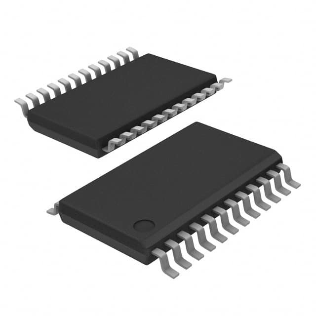
This PLL clock driver is available in a 24-pin TSSOP package, suitable for surface mount applications. It operates within a temperature range of 0°C to 70°C and requires a supply voltage between 3V and 3.6V.
The CDC2510BPWR has a nominal supply voltage of 3.3V, with a minimum of 3V and a maximum of 3.6V.
The CDC2510BPWR is supplied in a 24-TSSOP package.
The operating temperature range for the CDC2510BPWR is 0°C to 70°C.
The CDC2510BPWR operates from a minimum frequency of 25 MHz to a maximum frequency of 125 MHz.
The CDC2510BPWR has 10 outputs.
The typical supply current for the CDC2510BPWR is 10 uA.