

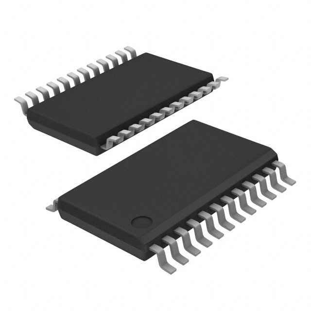
CDC2509BPWR The Texas Instruments CDC2509BPWR is a PLL Clock Driver designed for clock generation applications. It operates at 3.3V and features a frequency of 125MHz.
Mfr Part #:

CDC2509BPWR

Available from 1 distributors
Mfr Name: Texas Instruments
Texas Instruments
The Texas Instruments CDC2509BPWR is a PLL Clock Driver designed for clock generation applications. It operates at 3.3V and features a frequency of 125MHz.
Total Stock: 3,750 pcs

CDC2509BPWR Available from 1 distributor

Authorised
Non-Authorised
Distributor Stock Pricing MOQ PKG Lead Time Date Code On Order Quantity On Order Delivery
Non-Authorised Inventory information
3,750 pcs
3750 pcs On Request 1 On Request On Request 16+ On Request On Request

CDC2509BPWR Specifications Quick View

Most important parameters for selection – full specs in datasheet.
Category
Manufacturer Name
AEC Qualified
Automotive Grade
Differential
Divider
Frequency
Industrial Grade
Input
Lead Spacing
Lead Style
Medical Grade
Military Grade
Mounting Type
Number of Circuits
Operating Temperature
Output
PLL
Ratio
SVHC Present
Supplier Device Package
Supplier Package
Tape & Reel
Type
Voltage

CDC2509BPWR Description

Short technical summary and product information.

The Texas Instruments CDC2509BPWR is a PLL Clock Driver IC housed in a 24-TSSOP package. It operates within a voltage range of 3V to 3.6V and supports a frequency of 125MHz.


This component features a 1:9 clock ratio and utilizes LVTTL for both input and output signals. The PLL functionality includes a bypass mode. It is designed for surface mounting and operates within a temperature range of 0°C to 70°C.


The CDC2509BPWR is suitable for applications requiring precise clock signal generation and distribution. Its compact 24-TSSOP package makes it ideal for space-constrained designs.

CDC2509BPWR Quick Information

Product Type: Clock Generator, PLL, Frequency Synthesizer
Series: CDC2509
Canonical Name: Texas Instruments CDC2509BPWR PLL Clock Driver
Subcategory: PLL Clock Driver

CDC2509BPWR Compliance

RoHS Status: RoHS Compliant
Moisture Sensitivity Level (MSL): 1 Unlimited
REACH Status: REACH Unaffected
Lead Free: Yes

CDC2509BPWR Features

  • PLL Clock Driver IC
  • 3.3V operating voltage
  • 125MHz maximum frequency
  • 24-TSSOP surface mount package
  • LVTTL input and output signals

CDC2509BPWR Applications

  • Drives multiple clock signals from one source.
  • Provides a stable clock for digital systems.
  • Suitable for low-voltage digital applications.
  • Generates precise clock frequencies for timing.
  • Used in systems requiring clock signal distribution.

CDC2509BPWR FAQs

6 frequently asked questions generated from this part’s specifications.
What is the operating voltage for the CDC2509BPWR?

The operating voltage is 3V to 3.6V.

What is the maximum frequency of the CDC2509BPWR?

The maximum frequency is 125MHz.

What are the input and output signal types?

The input and output signal types are LVTTL.

What type of package is the CDC2509BPWR in?

It is in a 24-TSSOP package for surface mounting.

What is the operating temperature range?

The operating temperature range is 0°C to 70°C.

Does this PLL Clock Driver have a bypass function?

Yes, it has PLL functionality with a bypass option.

Home
Account

Categories