

| Distributor | Stock | Pricing | MOQ | PKG | Lead Time | Date Code | On Order Quantity | On Order Delivery | |
|---|---|---|---|---|---|---|---|---|---|
|
1,146 pcs
|
1146 pcs | On Request | 1 | On Request | On Request | 03+ | On Request | On Request |
| Category | |
| Manufacturer Name | |
| Differential | |
| Divider | |
| Frequency | |
| Input | |
| Mounting Type | |
| Number of Circuits | |
| Operating Temperature | |
| Output | |
| PLL | |
| Ratio | |
| Supplier Device Package | |
| Supplier Package | |
| Type | |
| Voltage |
The Texas Instruments CDC2509BPW is a PLL Clock Driver integrated circuit designed for clock generation and distribution applications. It operates at a nominal voltage of 3.3V, with a supply range of 3V to 3.6V. This device provides a frequency output of 125MHz and utilizes LVTTL logic for both its inputs and outputs.
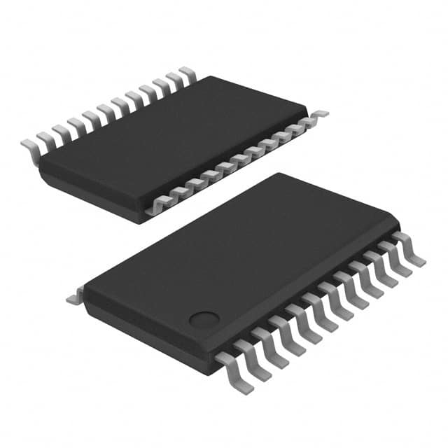
The CDC2509BPW features a 1:9 division ratio and includes PLL functionality with a bypass option. It is designed with a single circuit and operates within a temperature range of 0°C to 70°C. The component is housed in a 24-TSSOP package, measuring 0.173 inches (4.40mm) in width, and is intended for surface mount applications.
This clock driver is suitable for various electronic designs requiring precise clock signal generation and management. Its specifications make it a viable option for systems needing reliable clock synchronization and distribution.
The operating voltage is 3.3V.
The CDC2509BPW is available in a 24-TSSOP package.
The operating temperature range is 0°C to 70°C.
The output type is LVTTL.
The division ratio is 1:9.
Yes, it has PLL functionality with bypass.