
CD54HCT138F3A
Texas Instruments
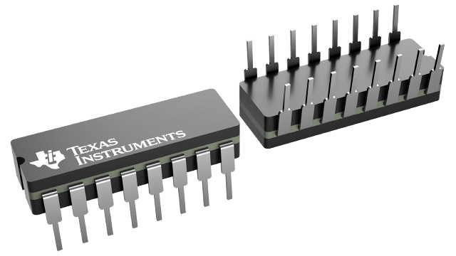
The Texas Instruments CD54HCT138F3A is a high-speed CMOS logic decoder/demultiplexer. It features a typical propagation delay of 13 ns and operates over a wide temperature range.


| Distributor | Stock | Pricing | MOQ | PKG | Lead Time | Date Code | On Order Quantity | On Order Delivery | |
|---|---|---|---|---|---|---|---|---|---|
|
7 pcs
|
7 pcs | On Request | 1 | On Request | On Request | On Request | On Request | On Request |
| Category | |
| Manufacturer Name | |
| Lead Style |
The Texas Instruments CD54HCT139F3A is a high-speed CMOS logic integrated circuit containing two independent binary to one of four decoders. Each decoder has a single active-low enable input. Data on the select inputs determine which of the four normally high outputs goes low. When the enable input is high, all outputs remain high. This device can function as a 1-to-4 line demultiplexer, with the enable input serving as the data input.
Designed for applications such as memory decoding, data routing, and code conversion, the CD54HCT139F3A offers multifunction capability. It supports HCT types with 4.5V to 5.5V operation and direct LSTTL input logic compatibility. The outputs can drive up to 10 LSTTL equivalent loads. The device operates across a wide temperature range of -55°C to 125°C.
Packaged in a 16-pin CDIP (J) format, this decoder/demultiplexer is suitable for various electronic designs requiring logic control and signal routing. Its balanced propagation delay and transition times contribute to efficient circuit performance.
| Qty | Low | High |
|---|---|---|
| 1+ | $22.27 | $22.27 |
Estimated market price range - modelled values for guidance only, not live distributor offers.
The CD54HCT139F3A operates over a temperature range of -55°C to 125°C.
The CD54HCT139F3A is available in a CDIP (J) package.
The CD54HCT139F3A has 2 channels.
The maximum supply current for the CD54HCT139F3A is 160 µA.
For HCT types, the input voltage range is 4.5V to 5.5V.
For HC types, the input voltage range is 2V to 6V.
The CD54HCT139F3A has direct LSTTL input logic compatibility, with VIL = 0.8V (Max) and VIH = 2V (Min).