

| Distributor | Stock | Pricing | MOQ | PKG | Lead Time | Date Code | On Order Quantity | On Order Delivery | |
|---|---|---|---|---|---|---|---|---|---|
|
21 pcs
|
21 pcs | On Request | 1 | On Request | On Request | On Request | On Request | On Request |
| Category | |
| Manufacturer Name | |
| Clock Frequency | |
| Features | |
| Input Type | |
| Military Grade | |
| Number of Channels | |
| Output Type | |
| Supply Current |
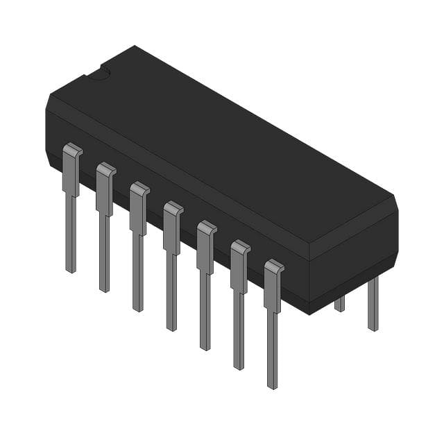
The Texas Instruments CD54HC107F3A is a high-speed CMOS logic device featuring dual negative-edge triggered J-K flip-flops with asynchronous reset. This component operates within the HC technology family and supports LVTTL/CMOS input types with push-pull outputs.
Key electrical specifications include a maximum clock frequency of 20 MHz, a maximum supply current of 80 µA, and output current capabilities of -6 mA (IOL) and 6 mA (IOH). The device offers high noise immunity, with N IL and N IH at 30% of V CC at 5V. It operates over a wide temperature range of -55°C to 125°C.
Designed for improved noise immunity and increased input rise and fall times, the CD54HC107F3A includes hysteresis on its clock inputs. It also features complementary outputs and buffered inputs. The device is available in a CDIP (J) package with a package area of 130.4652 mm².
This flip-flop is suitable for various digital logic applications requiring reliable state storage and clocking. Its military rating and wide operating temperature range make it suitable for demanding environments.
| Qty | Low | High |
|---|---|---|
| 1+ | $13.27 | $13.27 |
Estimated market price range - modelled values for guidance only, not live distributor offers.
For HC types, the operating voltage range is 2V to 6V. For HCT types, the range is 4.5V to 5.5V.
It is available in a CDIP (J) 14-pin ceramic dual-inline package.
The operating temperature range is -55°C to +125°C.
The typical maximum clock frequency is 60 MHz at VCC=5V, CL=15pF, TA=25°C.
Standard outputs can drive up to 10 LSTTL loads; bus driver outputs can drive up to 15 LSTTL loads.
It is compatible with CMOS and LSTTL logic; VIL max 0.8V, VIH min 2V for LSTTL.
IOL (max) is -6 mA and IOH (max) is 6 mA.