

| Distributor | Stock | Pricing | MOQ | PKG | Lead Time | Date Code | On Order Quantity | On Order Delivery | |
|---|---|---|---|---|---|---|---|---|---|
|
19 pcs
|
19 pcs | On Request | 1 | On Request | On Request | On Request | On Request | On Request |
| Category | |
| Manufacturer Name | |
| Clock Frequency | |
| Input Type | |
| Lead Style | |
| Number of Channels | |
| Operating Temperature Range | |
| Output Type | |
| Supply Current | |
| Supply Voltage |
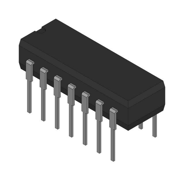
The CD54AC74F3A from Texas Instruments is a dual positive-edge-triggered D-type flip-flop. This component belongs to the AC technology family and utilizes standard CMOS input and push-pull output types.
Key electrical specifications include a maximum clock frequency of 110 MHz, an IOL of 24 mA, and an IOH of -24 mA. The device has a maximum supply current of 80 µA and supports a supply voltage range of 1.5V to 5.5V. It offers balanced outputs and high speed with propagation delays typically between 10-50 ns.
Designed for robust performance, the CD54AC74F3A operates across a wide temperature range from -55°C to 125°C. It features positive input clamp diodes and is built on a SCR-latchup-resistant CMOS process. The output drive current is ±24 mA, allowing for a fanout to 15 F devices.
This flip-flop is packaged in a CDIP (J) format with a package area of 130.4652 mm². Its design considerations include balanced noise immunity and reduced power consumption compared to bipolar logic families.
| Qty | Low | High |
|---|---|---|
| 1+ | $10.49 | $10.49 |
Estimated market price range - modelled values for guidance only, not live distributor offers.
The supply voltage range for the CD54AC74F3A is 1.5 V to 5.5 V.
The operating temperature range for the CD54AC74F3A is -55 to 125 °C.
The package type for the CD54AC74F3A is CDIP (J).
The CD54AC74F3A has 2 channels.
The maximum clock frequency of the CD54AC74F3A is 110 MHz.
The output drive current of the CD54AC74F3A is ±24 mA.
The maximum supply current for the CD54AC74F3A is 80 µA.