

| Distributor | Stock | Pricing | MOQ | PKG | Lead Time | Date Code | On Order Quantity | On Order Delivery | |
|---|---|---|---|---|---|---|---|---|---|
|
40,000 pcs
|
40000 pcs | On Request | 1 | On Request | On Request | On Request | On Request | On Request | |
|
139 pcs
|
139 pcs | On Request | 1 | On Request | On Request | On Request | On Request | On Request | |
|
139 pcs
|
139 pcs | On Request | 1 | On Request | On Request | On Request | On Request | On Request |
| Category | |
| Manufacturer Name | |
| Current | |
| Features | |
| Input Logic Level | |
| Input Voltage | |
| Logic Type | |
| Max Propagation Delay @ V, Max CL | |
| Mounting Type | |
| Number of Circuits | |
| Number of Inputs | |
| Operating Temperature | |
| Supplier Device Package | |
| Supply Voltage | |
| Voltage |
The CD4093BCN from On Semiconductor is a versatile integrated circuit featuring four independent 2-input NAND gates, each equipped with Schmitt-trigger functionality on its inputs. This design provides superior noise immunity and ensures reliable switching characteristics across a wide supply voltage range of 3V to 15V.
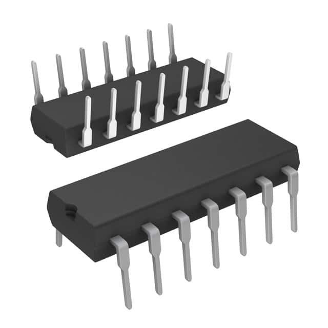
The device operates reliably in extreme temperatures, with an operating temperature range of -55°C to 125°C, making it suitable for demanding environments. The CD4093BCN is packaged in a standard 14-pin Dual In-line Package (DIP) with a 0.300" width, designed for through-hole mounting.
Key features include Schmitt-trigger action on each input, which allows for clean signal transitions even in the presence of noise. The NAND logic type and the presence of four independent circuits make it adaptable for various digital logic applications, including wave shaping, pulse generation, and high-noise-environment systems. Its standard B-series output drive ensures compatibility with other logic families.
| Qty | Low | High |
|---|---|---|
| 1+ | $0.22 | $0.22 |
Estimated market price range - modelled values for guidance only, not live distributor offers.
The CD4093BCN operates from 3V to 15V supply voltage.
The operating temperature range is -55°C to 125°C.
It is available in a 14-DIP (0.300", 7.62mm) through-hole package, also known as 14-MDIP.
It implements a NAND gate function.
It contains 4 circuits, each with 2 inputs.
Typical quiescent current is 0.25µA at VDD = 5V.
Maximum propagation delay is 160ns at VDD = 15V and CL = 50pF.