

| Distributor | Stock | Pricing | MOQ | PKG | Lead Time | Date Code | On Order Quantity | On Order Delivery | |
|---|---|---|---|---|---|---|---|---|---|
|
258 pcs
|
258 pcs | On Request | 1 | On Request | On Request | 17+ | On Request | On Request |
| Category | |
| Manufacturer Name | |
| Lead Style | |
| Operating Temperature Range | |
| Operating Voltage | |
| Package Quantity | |
| Propagation Delay | |
| SVHC Present |
The CD4082BF3A from Texas Instruments is a high-reliability, military-grade dual 4-input AND gate. This CMOS device is designed for operation across a wide voltage supply range, from 3 V to 18 V. It offers medium-speed operation with typical propagation delays of 60 ns at 10 V.
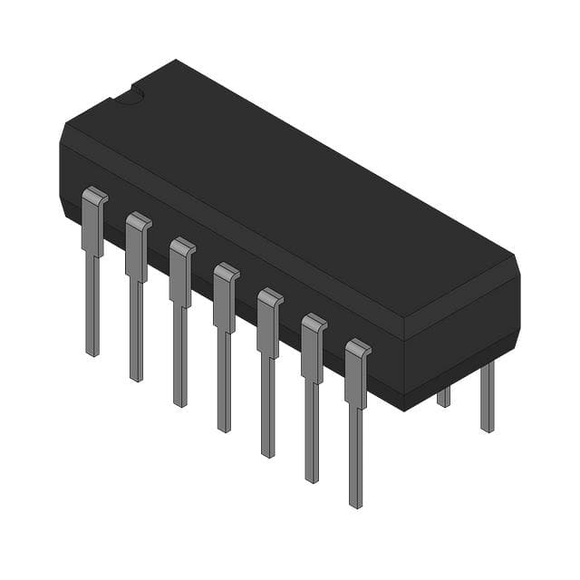
The CD4082BF3A is specified for operation in harsh environments, with an extended operating temperature range of -55°C to 125°C. It features standardized, symmetrical output characteristics and meets JEDEC specifications for B-Series CMOS devices. The component is housed in a 14-pin CDIP package, suitable for through-hole mounting.
Key electrical characteristics include a maximum input current of 1 µA at 18 V over the full temperature range and specific noise margin values at different supply voltages (1 V at 5 V, 2 V at 10 V, and 2.5 V at 15 V). This makes it a robust choice for various digital logic applications requiring reliable AND gate functionality.
| Qty | Low | High |
|---|---|---|
| 1+ | $10.27 | $10.27 |
Estimated market price range - modelled values for guidance only, not live distributor offers.
3 V to 18 V.
14-pin CDIP (J) package, supplied in tube.
-55°C to 125°C.
60 ns at V_DD = 10 V.
1 µA at 18 V over full package temperature range, and 100 nA at 18 V and 25°C.
Minimum of 1 V at V_DD = 5 V, 2 V at V_DD = 10 V, and 2.5 V at V_DD = 15 V.
25 units per tube.