

| Distributor | Stock | Pricing | MOQ | PKG | Lead Time | Date Code | On Order Quantity | On Order Delivery | |
|---|---|---|---|---|---|---|---|---|---|
|
1,036 pcs
|
1036 pcs | On Request | 1 | On Request | On Request | 230 | On Request | On Request |
| Category | |
| Manufacturer Name | |
| Current | |
| Input Logic Level | |
| Logic Type | |
| Max Propagation Delay @ V, Max CL | |
| Mounting Type | |
| Number of Circuits | |
| Number of Inputs | |
| Operating Temperature | |
| SVHC Present | |
| Supplier Device Package | |
| Voltage |
The CD4069UBCSJX from ON Semiconductor is a CMOS inverter circuit designed for broad applicability in digital logic systems. It comprises six independent inverter gates, each capable of performing a single-input inversion function.
This device supports a wide operating supply voltage range from 3V to 15V, making it suitable for various power environments. It exhibits high noise immunity and low power consumption characteristic of CMOS technology. The operating temperature range is specified from -55°C to +125°C, ensuring reliable performance in demanding conditions.
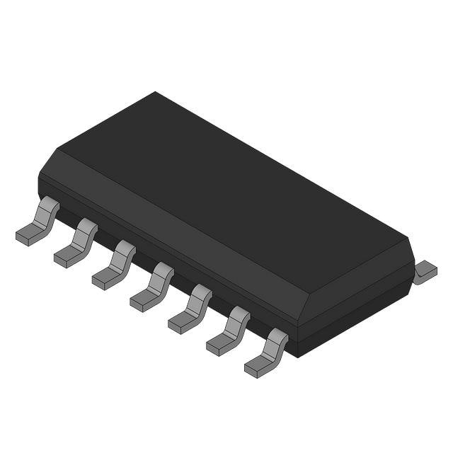
Packaged in a 14-lead Small Outline Package (SOP), the CD4069UBCSJX is designed for surface mounting. Its input pins are protected against static discharge by internal diode clamps. This inverter is equivalent to the MM74C04 and is intended for general-purpose inverter applications where specialized buffer characteristics are not required.
Key electrical characteristics include a maximum propagation delay of 50ns at 15V and 50pF. The low output voltage is typically 0.05V, and the high output voltage is close to the supply voltage. Quiescent current is very low, typically 0.25µA at 5V.
| Qty | Low | High |
|---|---|---|
| 1+ | $0.22 | $0.22 |
Estimated market price range - modelled values for guidance only, not live distributor offers.
The CD4069UBCSJX operates from 3V to 15V.
The CD4069UBCSJX is supplied in a 14-SOP package.
The operating temperature range for the CD4069UBCSJX is -55°C to 125°C.
The RoHS status is RoHS3 Compliant.
The CD4069UBCSJX contains six inverter circuits.
The maximum propagation delay is 50ns at 15V and 50pF.