

| Distributor | Stock | Pricing | MOQ | PKG | Lead Time | Date Code | On Order Quantity | On Order Delivery | |
|---|---|---|---|---|---|---|---|---|---|
|
2,764 pcs
|
2764 pcs | On Request | 1 | On Request | On Request | On Request | On Request | On Request | |
|
32 pcs
|
32 pcs | On Request | 1 | On Request | On Request | On Request | On Request | On Request |
| Category | |
| Manufacturer Name | |
| Current | |
| Input Logic Level | |
| Logic Type | |
| Max Propagation Delay @ V, Max CL | |
| Mounting Type | |
| Number of Circuits | |
| Number of Inputs | |
| Operating Temperature | |
| Supplier Device Package | |
| Supplier Package | |
| Voltage |
The CD4049UBD from Texas Instruments is a versatile 6-channel inverting hex buffer. It is designed to function as a CMOS to DTL or TTL converter, capable of driving up to two DTL or TTL loads directly. This device operates over a wide voltage range of 3V to 18V, making it suitable for various applications.
The CD4049UBD features a single input per gate and provides an inverted output. Its input logic levels can exceed the VCC supply voltage, which is beneficial for logic-level conversions. The device is specified for an operating temperature range of -55°C to 125°C.
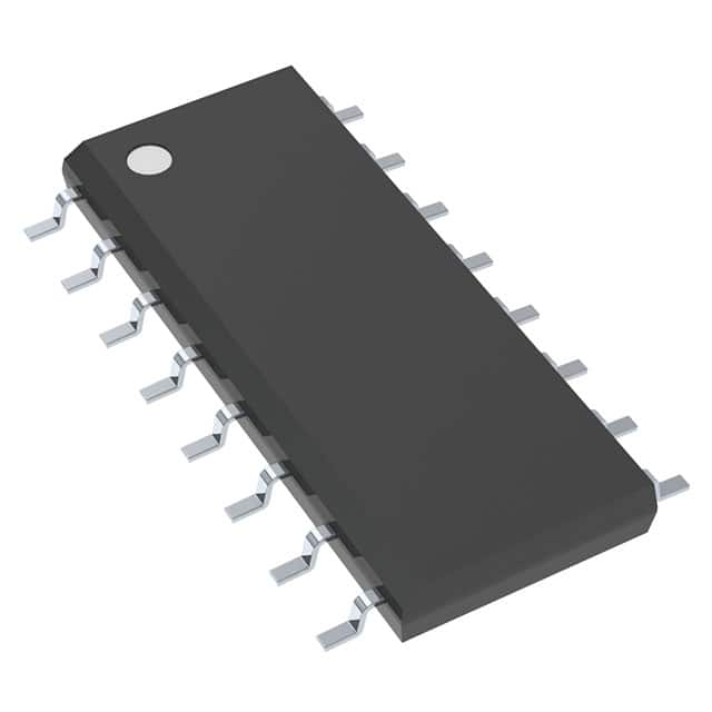
Packaged in a 16-SOIC (Surface Mount) configuration, the CD4049UBD is designed for easy integration into printed circuit boards. Its high sink current capability and wide operating voltage make it a reliable choice for signal buffering and level shifting tasks in digital circuits.
| Qty | Low | High |
|---|---|---|
| 1+ | $0.46 | $0.46 |
Estimated market price range - modelled values for guidance only, not live distributor offers.
The CD4049UBD operates from 3V to 18V.
The CD4049UBD is available in a 16-SOIC surface mount package.
The CD4049UBD operates from -55°C to 125°C.
The CD4049UBD is an inverter logic gate.
The CD4049UBD contains six inverter circuits.
The input logic high level is minimum 4V and logic low level is maximum 12.5V.
The maximum propagation delay is 50ns at 15V supply and 50pF load.