

| Distributor | Stock | Pricing | MOQ | PKG | Lead Time | Date Code | On Order Quantity | On Order Delivery | |
|---|---|---|---|---|---|---|---|---|---|
|
3,600 pcs
|
3600 pcs | On Request | 1 | On Request | On Request | On Request | On Request | On Request | |
|
875 pcs
|
875 pcs | On Request | 1 | On Request | On Request | 1111 | On Request | On Request | |
|
450 pcs
|
450 pcs | On Request | 1 | On Request | On Request | On Request | On Request | On Request |
| Category | |
| Manufacturer Name | |
| Current | |
| Current - Quiescent (Max) | |
| Input Logic Level | |
| Logic Type | |
| Max Propagation Delay @ V, Max CL | |
| Mounting Type | |
| Number of Circuits | |
| Number of Inputs | |
| Operating Temperature | |
| Supplier Device Package | |
| Voltage | |
| Voltage Supply |
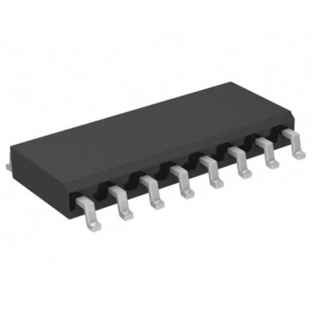
The CD4049UBCM from ON Semiconductor is a monolithic complementary MOS (CMOS) integrated circuit functioning as a hex inverter. It is constructed with N- and P-channel enhancement mode transistors and is designed for logic level conversion using a single supply voltage.
This device features a wide supply voltage range of 3V to 15V and can directly drive two DTL/TTL loads at 5.0V. It offers high source and sink current capability. The input protection allows input voltages to exceed the VDD supply, making it suitable for CMOS to DTL/TTL conversion.
Key electrical characteristics include a maximum propagation delay of 35ns at 15V with a 50pF load. It has 6 independent inverter circuits, each with a single input. The operating temperature range is -55°C to 125°C.
The CD4049UBCM is available in a 16-SOIC surface-mount package, specifically the 16-SOIC (0.154", 3.90mm Width) configuration. It is suitable for applications requiring CMOS hex buffering, CMOS to DTL/TTL hex conversion, or CMOS current sink/source driving.
| Qty | Low | High |
|---|---|---|
| 1+ | $0.22 | $0.22 |
Estimated market price range - modelled values for guidance only, not live distributor offers.
3V to 15V.
16-SOIC surface mount package.
-55°C to 125°C.
6.
Inverter.
35ns at 15V, 50pF.
High: 4V to 12V, Low: 1V to 2.5V.